System including a buffered memory module

a memory module and buffer technology, applied in the field of integrated circuit devices, can solve the problems of adversely affecting the rate at which dram technology can keep pace with the increasing data bandwidth and system capacity requirements, and is difficult to keep up with the increasing data bandwidth and system memory requirements

Active Publication Date: 2007-04-19
RAMBUS INC
View PDF99 Cites 162 Cited by
  • Summary
  • Abstract
  • Description
  • Claims
  • Application Information

AI Technical Summary

Problems solved by technology

There are several major trends in dynamic random access memory (“DRAM”) that may make it costly and challenging to keep up with increasing data bandwidth and system memory requirements.
For example, transistor speed relative to feature size improvements in a given DRAM technology node, and the rising costs of capital investment required to move DRAM technology to greater memory densities for a given DRAM die adversely affect the rate at which DRAM technology can keep pace with the increasing data bandwidth and system capacity requirements.

Method used


Image

  • System including a buffered memory module
  • System including a buffered memory module
  • System including a buffered memory module

Examples


Embodiment Construction

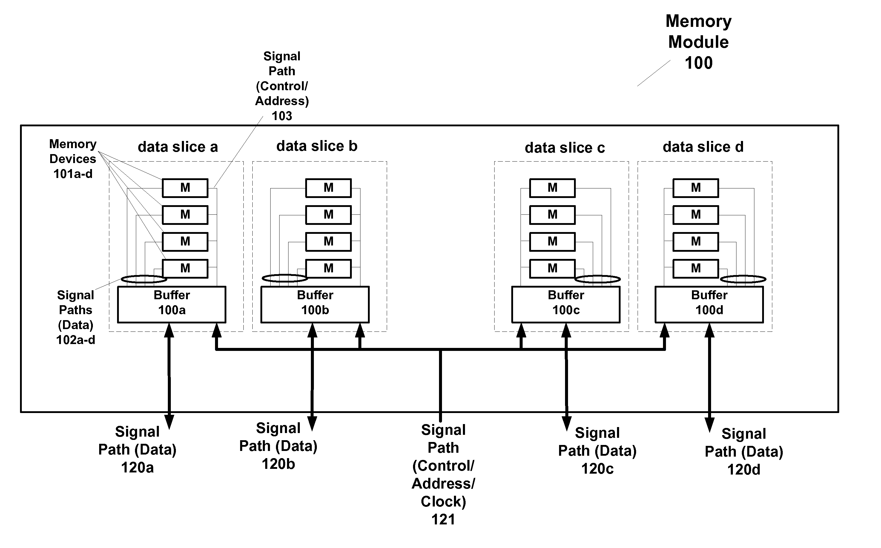
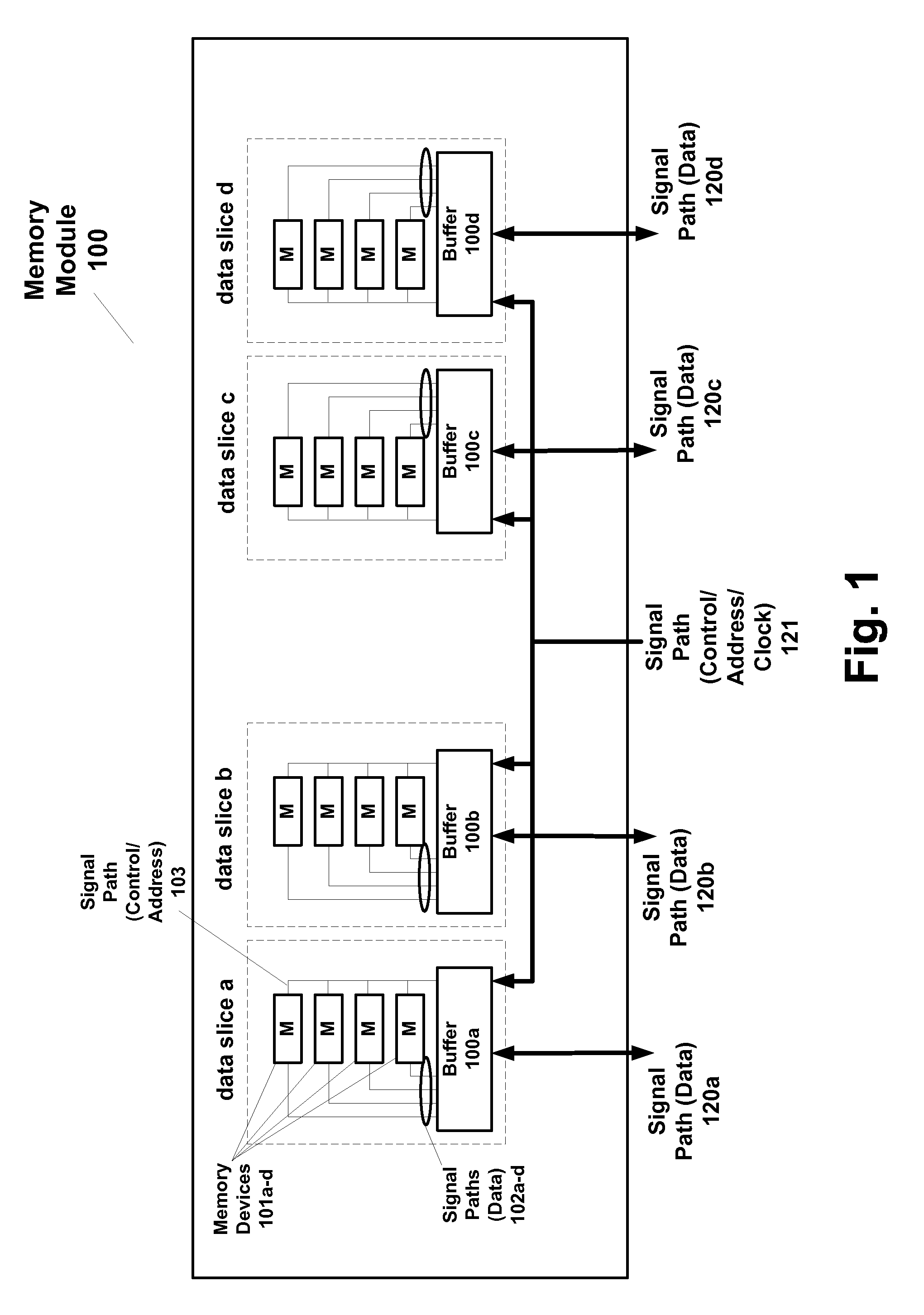
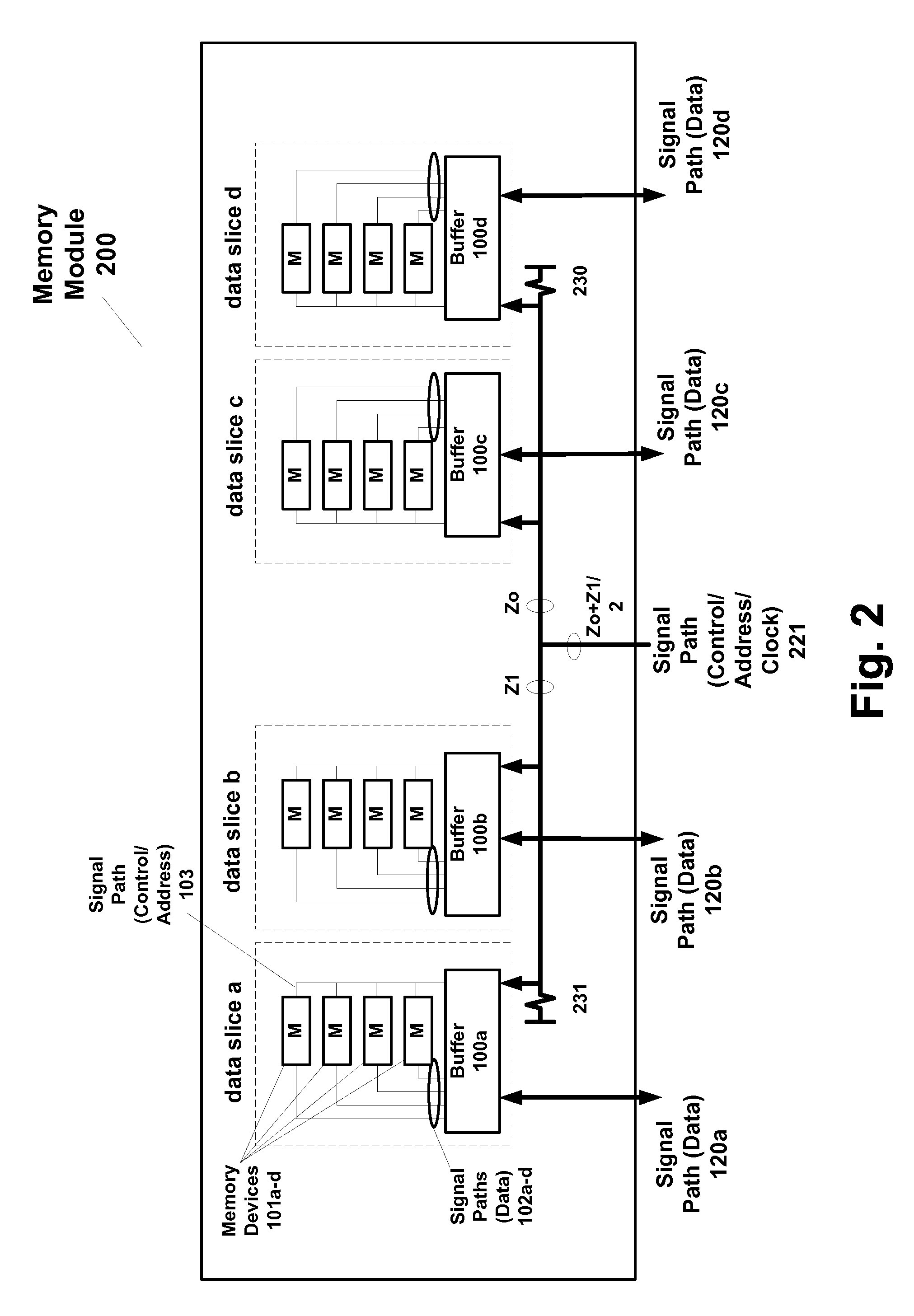
[0037] According to embodiments, a system includes a master device and a first memory module having a plurality of integrated circuit memory devices and a plurality of integrated circuit buffer devices that operate in first and second modes of operation (bypass mode). In a first mode of operation, a first memory module provides read data from the plurality of integrated circuit memory devices (via an integrated circuit buffer device) on a first signal path to the master and a second memory module simultaneously provides read data from its plurality of integrated circuit memory devices (via another integrated circuit buffer device on the second module) on a third signal path coupled to the master device. In a second mode of operation, the first memory module provides first read data from its plurality of integrated circuit memory devices (via the integrated circuit buffer device) on the first signal path and second read data from its plurality of integrated circuit memory devices (vi...


PUM


Abstract

According to embodiments, a system includes a master device and a first memory module having a plurality of integrated circuit memory devices and a plurality of integrated circuit buffer devices that operate in first and second modes of operation (bypass mode). In a first mode of operation, a first memory module provides read data from the plurality of integrated circuit memory devices (via a integrated circuit buffer device) on a first signal path to the master and a second memory module simultaneously provides read data from its plurality of integrated circuit memory devices (via another integrated circuit buffer device on the second module) on a third signal path coupled to the master device. In a second mode of operation, the first memory module provides first read data from its plurality of integrated circuit memory devices (via the integrated circuit buffer device) on the first signal path and second read data from its plurality of integrated circuit memory devices (via the integrated circuit buffer device) on a second signal path that is coupled to a second memory module. An integrated circuit buffer device in the second memory module then bypasses the second read data from the second signal path and provides the second read data on a third signal path coupled to the master device.

Description

RELATED APPLICATION [0001] This application is a continuation-in-part of U.S. patent application Ser. No. 11 / 236,401 filed on Sep. 26, 2005 (still pending).FIELD OF THE INVENTION [0002] The present invention generally relates to integrated circuit devices, high speed signaling of such devices, memory devices, and memory systems. BACKGROUND [0003] Some contemporary trends predict that processors, such as general purpose microprocessors and graphics processors, will continue to increase system memory and data bandwidth requirements. Using parallelism in applications such as multi-core processor architectures and multiple graphics pipelines, processors should be able to drive increases in system bandwidths at rates some predict will be doubled every three years for the next ten years. There are several major trends in dynamic random access memory (“DRAM”) that may make it costly and challenging to keep up with increasing data bandwidth and system memory requirements. For example, trans...

Claims


Application Information

Patent Timeline
Patent Type & Authority Applications(United States)
IPC IPC(8): G01R31/28
CPCG11C5/02G11C5/04G11C5/063G11C11/4093G11C2029/4402H01L2224/16225H01L2224/32145H01L2224/32225H01L2224/48091H01L2224/48227H01L2224/73253H01L2224/73265H01L2924/15182H01L2924/15192H01L2924/15311H01L2924/15331H01L2224/48095H01L24/73H01L2924/14H01L2924/00012H01L2924/00H01L2924/00014
Inventor TSERN, ELYSHAEFFER, IANHAMPEL, CRAIG
Owner RAMBUS INC
Why Eureka
Try Eureka