Sensor having semiconductor chip and circuit chip

Inactive Publication Date: 2007-04-26
DENSO CORP
View PDF4 Cites 21 Cited by
  • Summary
  • Abstract
  • Description
  • Claims
  • Application Information

AI Technical Summary

Benefits of technology

[0010] In the above device, the semiconductor chip is sandwiched between the first and second films. Therefore, both interfaces between the semiconductor chip and the first and second films have stress. The stress is caused by a difference of linear coefficient of expansion between the semiconductor chip and the first or second film. Accordingly, deformation of the semiconductor chip caused by the difference of linear coefficient of expansion is reduced.
[0012] In the above device, the semiconductor chip is sandwiched between the first and second films. Therefore, both interfaces between the semiconductor chip and the first and second films have stress. The stress is caused by a difference of linear coefficient of expansion between the semiconductor chip and the first or second film. Accordingly, deformation of the semiconductor chip caused by the difference of linear coefficient of expansion is reduced.

Problems solved by technology

If foreign substances are adhered with respect to these sensing portions when bump connections are performed, there is such a risk that sensing characteristics of these sensing portions are largely varied.
However, there is a large difference between linear expansion coefficients as to a semiconductor chip, which is made of a semiconductor such as silicon, and a film, which is made of a resin.
In other words, the temperature characteristics of the sensors may be deteriorated due to the temperature cycle.

Method used


Image

  • Sensor having semiconductor chip and circuit chip
  • Sensor having semiconductor chip and circuit chip
  • Sensor having semiconductor chip and circuit chip

Examples


first embodiment

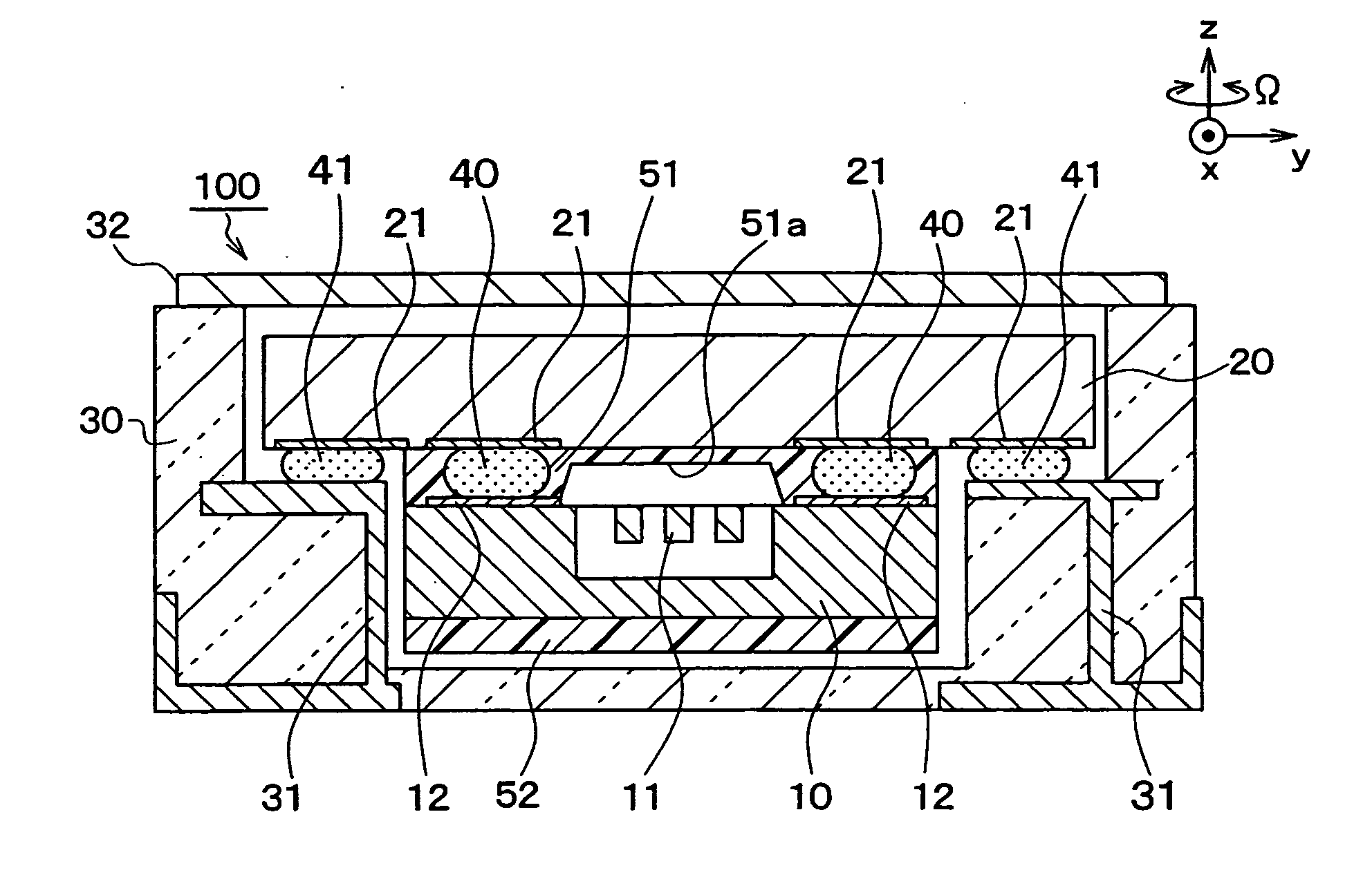
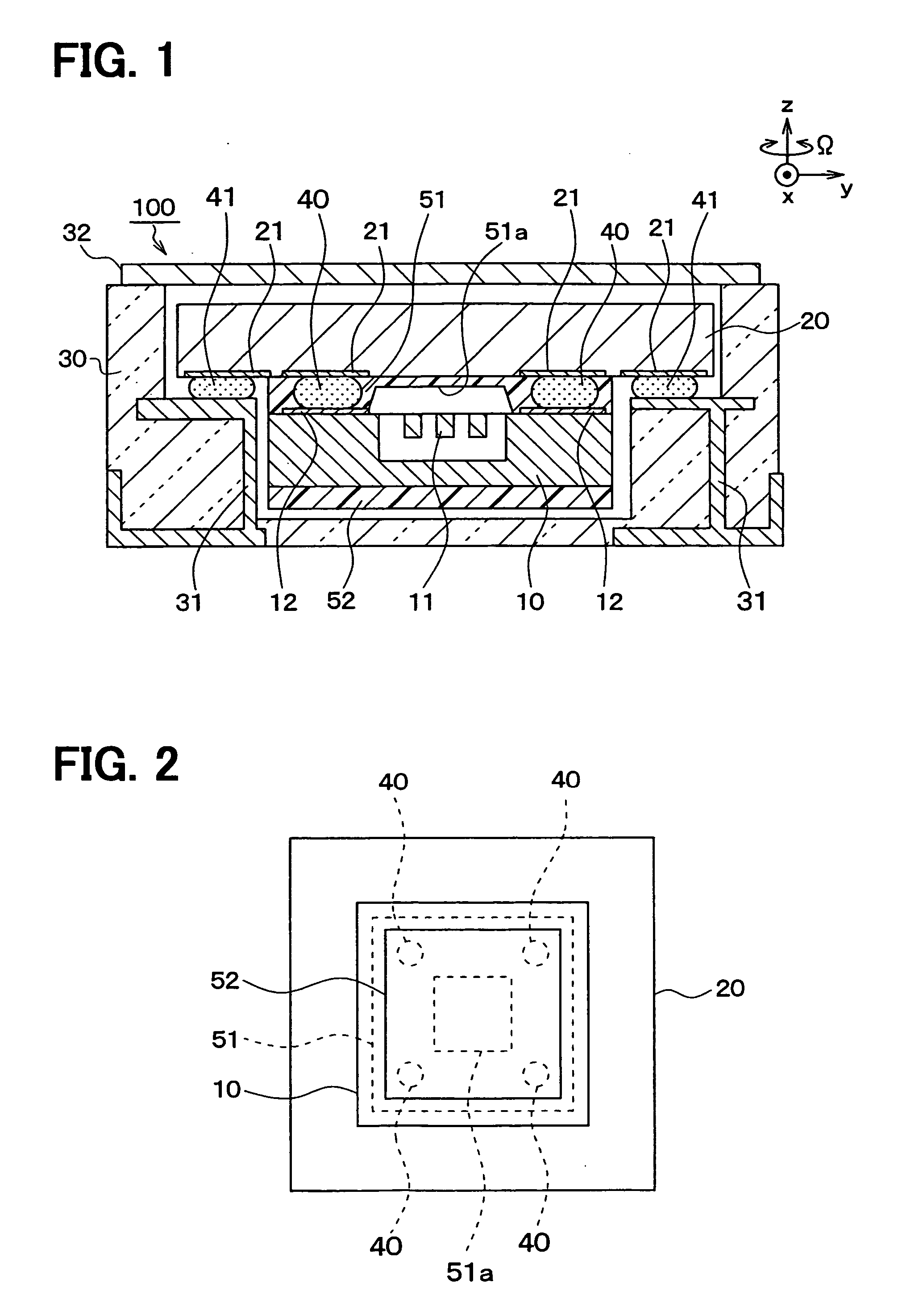
[0022] As indicated in FIG. 1, the angular velocity sensor apparatus 100 of this first embodiment has been mainly constituted by employing a sensor chip 10 as a semiconductor chip, a circuit chip 20, and a package 30 for storing the sensor chip 10 and the circuit chip 20 thereinto.

[0023] In this first embodiment, the sensor chip 10 has been constructed as the semiconductor chip for sensing angular velocities as physical quantity. A vibrator member 11 has been provided on the side of one plane of this sensor chip 10, while the vibrator member 11 corresponds to a sensing portion as well as a movable portion.

[0024] Such a sensor chip 10 is formed in such a manner that, for example, the micromachine processing operation which is well known in the technical field is carried out with respect to a semiconductor substrate, for instance, an SOI (silicon-on-insulator) substrate. In this first embodiment, the sensor chip 10 is made in a rectangular plate shape as shown in FIG. 2.

[0025] Concr...

second embodiment

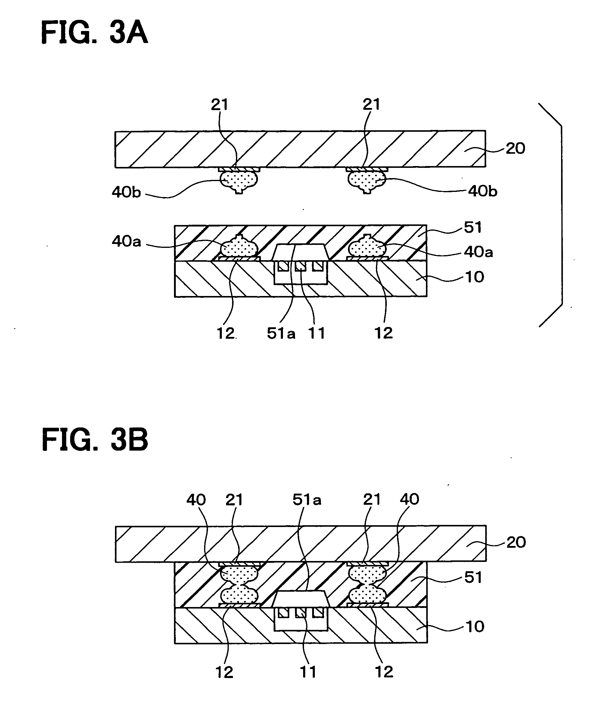
[0091] As explained in this second embodiment, the second film 52 is separated from the sensor chip 10 at the same portion as the first film 51. As a result, the joining areas of these first and second films 51 and 52, and also the patterns of the joining regions can be resembled to each other as being permitted as possible.

[0092] More specifically, as explained in this example, both the first film 51 and the second film 52 may have the same concave shapes, so that the joining areas and the patterns of the joining regions in the first film 51 and the second film 52 can be made equal to each other.

[0093] Also, in order to make the joining areas and the patterns of the joining regions as to the first and second films 51 and 52 equal to each other, the film shapes of both the first and second films 51 and 52 may not be identical to each other; may be different from each other; or the sizes of these first and second films 51 and 52 may be different from each other. For instance, the ad...

third embodiment

[0097] To the contrary, as explained in this third embodiment, in the circuit chip 20, the third film 53 made of the resin is joined on not only one plane of this circuit chip 20, but also the other plane thereof located opposite to one plane. As a result, the circuit chip 20 owns stresses on both the planes thereof due to a difference in linear expansion coefficients between the circuit chip 20 and the first film 51.

[0098] As a result, in accordance with this third embodiment, the deformations of the circuit chip 20 caused by the difference in the linear expansion coefficients can be suppressed. Thus, the deformations of the circuit chip 20 may be suppressed, which may conduct to prevent the deformation of the sensor chip 10.

[0099] Also, as explained in this third embodiment, in such a case that the first film 51 and the third film 53 which are made of the resin are joined to both the planes of the circuit chip 20, these first and third films 51 and 53 may be made of the same mate...


PUM


Abstract

A sensor includes: a semiconductor chip having a sensing portion; a circuit chip; and first and second films. The sensing portion is disposed on a first side of the semiconductor chip. The first side of the semiconductor chip is electrically connected to the circuit chip through a bump. The first side of the semiconductor chip faces the circuit chip. The first film is disposed on the first side of the semiconductor chip. The first film covers the sensing portion, and is made of resin, and the second film is made of resin, and disposed on a second side of the semiconductor chip.

Description

CROSS REFERENCE TO RELATED APPLICATION [0001] This application is based on Japanese Patent Application No. 2005-307031 filed on Oct. 21, 2005, the disclosure of which is incorporated herein by reference. FIELD OF THE INVENTION [0002] The present invention relates to a sensor having a semiconductor chip and a circuit chip. BACKGROUND OF THE INVENTION [0003] Conventionally, various sensor apparatus have been proposed (refer to, for example, JP-A-2001-217280). That is, in a conventional sensor apparatus, when a semiconductor chip having a sensing portion on one plane of this semiconductor chip is electrically connected to a circuit chip, the semiconductor chip and the circuit chip are stacked on each other, and then, a bump is interposed between these semiconductor chip and circuit chip so as to electrically connect these chips with each other. The sensing portion of the semiconductor chip senses physical quantity such as angular velocities, acceleration, and pressure. [0004] While the...

Claims


Application Information

Patent Timeline
IPC IPC(8): H01L23/48G01C19/00H01L21/60H01L25/065H01L25/07H01L25/16H01L25/18H01L29/84
CPCB81C1/0023G01C19/5719G01P1/023H01L2224/16H01L2924/01079H01L2924/13091H01L2924/1305H01L2924/01068H01L2924/00H01L2224/05573H01L2224/05568H01L2224/05624H01L2224/06135H01L24/05H01L2924/00014
Inventor SAKAI, MINEKAZUABE, RYUICHIRONINOMIYA, YASUNORI
Owner DENSO CORP
Why Eureka
Try Eureka