Electronic component, module, module assembling method, module identification method and module environment setting method

a technology of electronic components and modules, applied in the direction of electrical apparatus, semiconductor devices, semiconductor/solid-state device details, etc., can solve the problems of excessive time and effort, and achieve the effect of favorable modules

Inactive Publication Date: 2007-05-03
SHARP KK +2
View PDF7 Cites 38 Cited by
  • Summary
  • Abstract
  • Description
  • Claims
  • Application Information

AI Technical Summary

Benefits of technology

[0067] According to the invention, it is possible to set operation environments in the semiconductor devices of a m

Problems solved by technology

There is no problem in the case of stacking different kinds of chips because the chips have different configurations originally, but, for example, in the case of realizing a large-capacity memory by stacking a large number of memory chips, it is necessary to produce the same number of

Method used


Image

  • Electronic component, module, module assembling method, module identification method and module environment setting method
  • Electronic component, module, module assembling method, module identification method and module environment setting method
  • Electronic component, module, module assembling method, module identification method and module environment setting method

Examples


Embodiment Construction

[0095] Now referring to the drawings, preferred embodiments of the invention are described below.

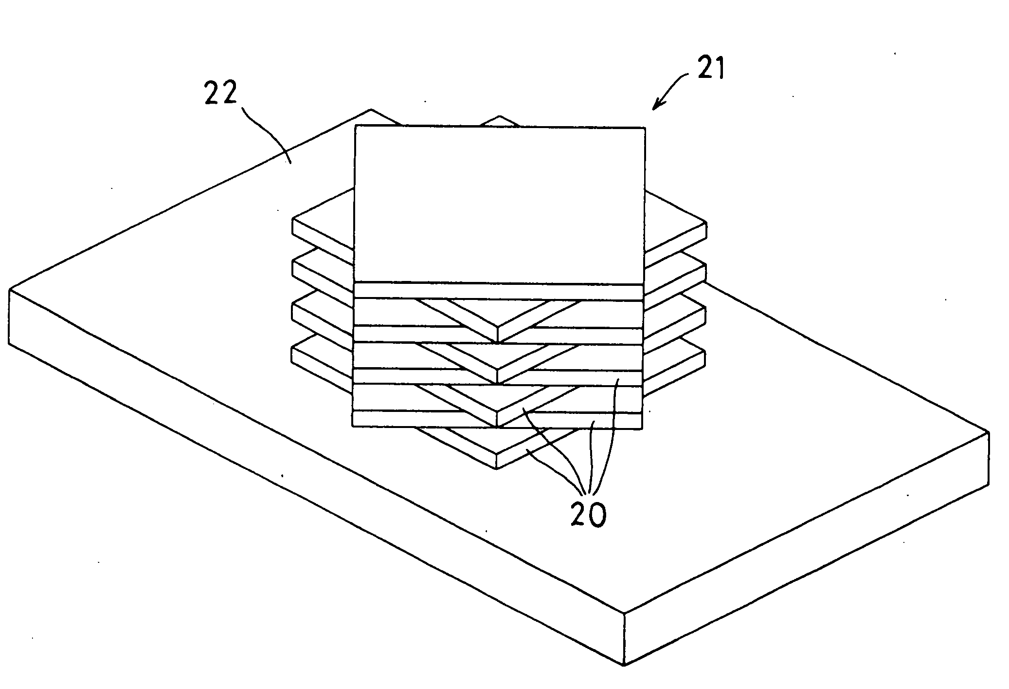
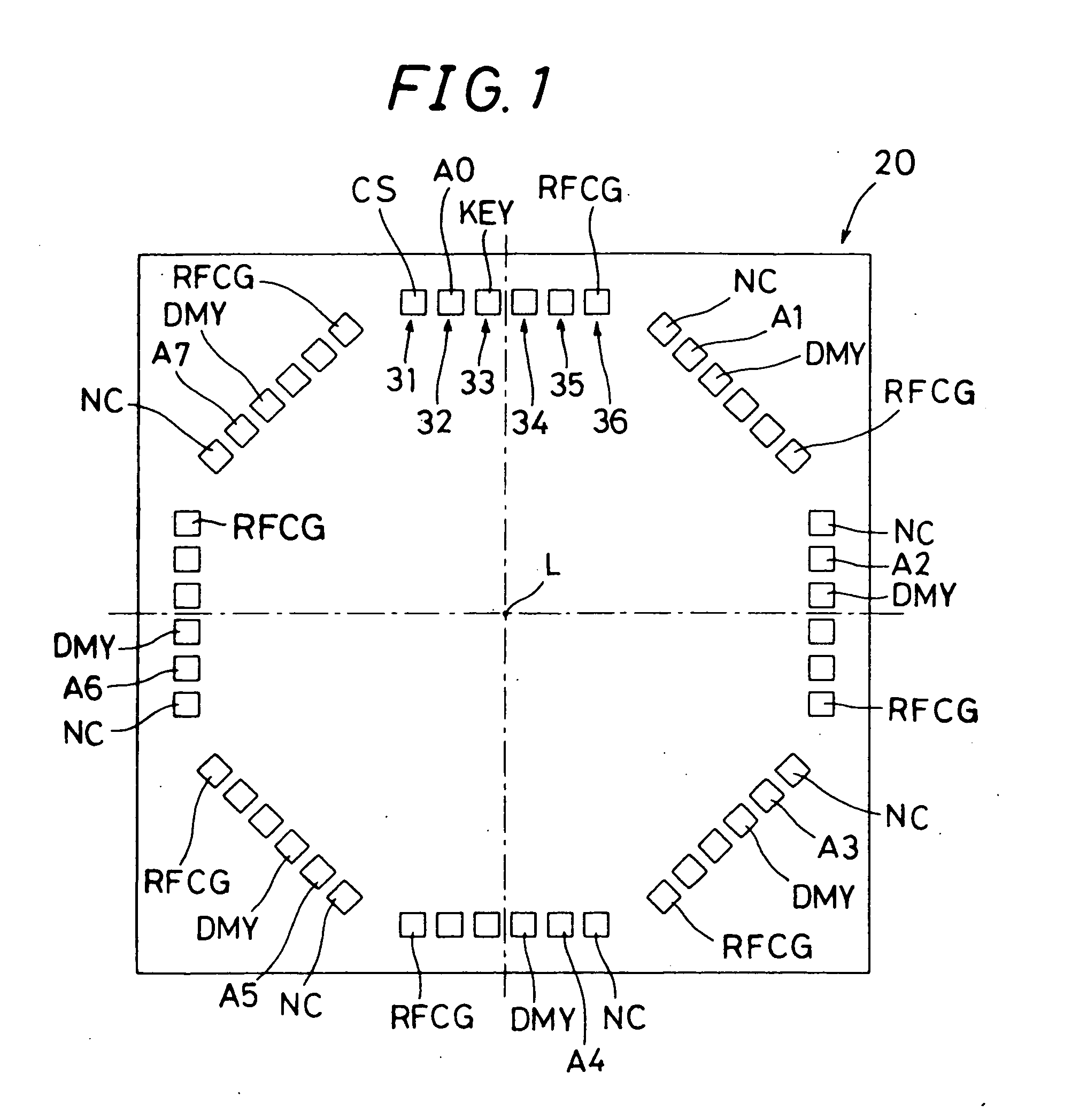
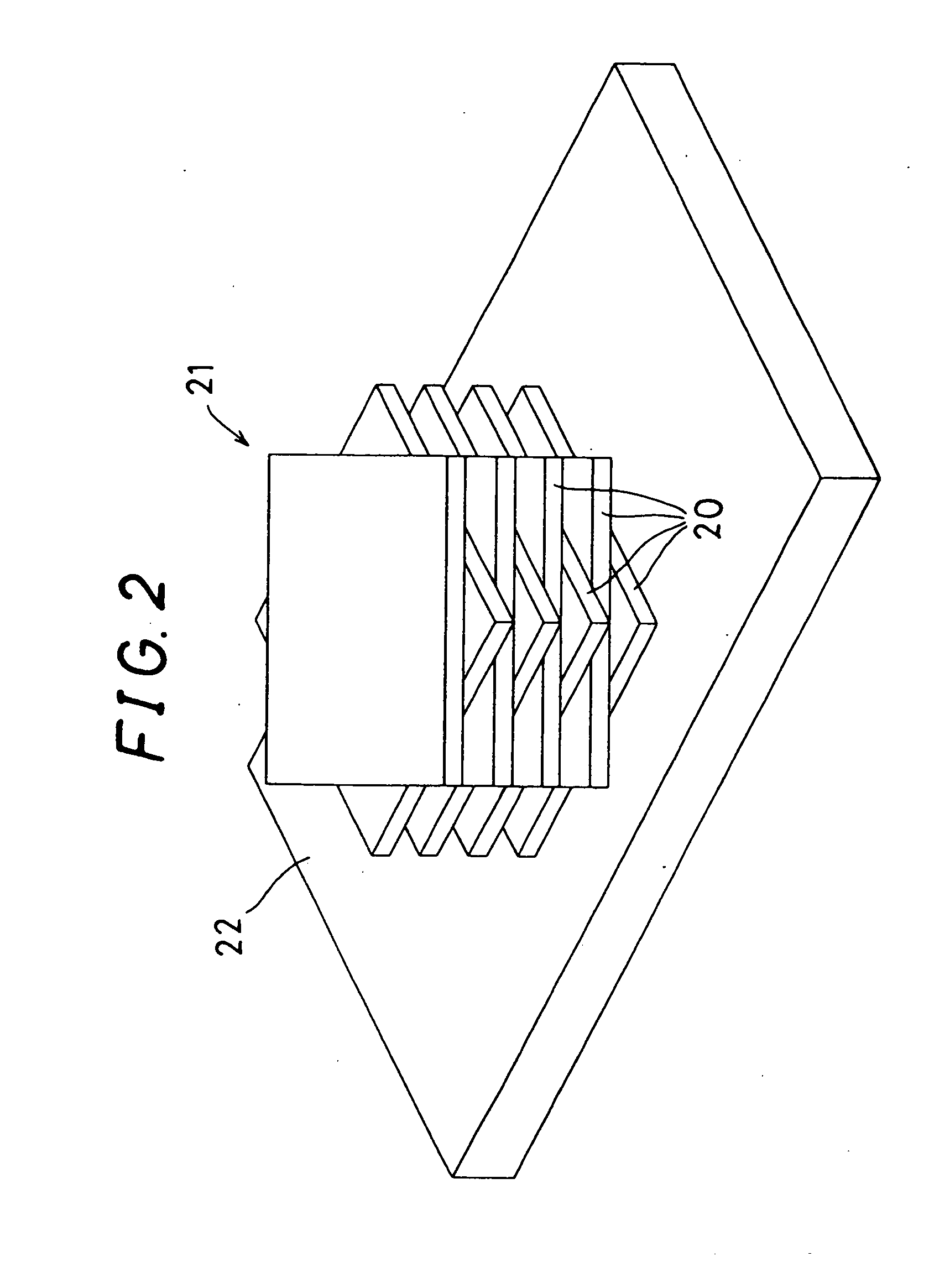
[0096]FIG. 1 is a front view showing a memory chip 20 according to an embodiment of the invention. FIG. 2 is a perspective view showing a memory module 21 assembled by using the memory chips 20 in a state mounted on a board 22. The memory chip (occasionally referred to as “chip” hereinafter) 20 is an electronic component, and used for assembling the memory module (occasionally referred to as “module” hereinafter) 21, which is high-capacitance and small-sized, by stacking a plurality of chips 20 in order to realize high-density packaging.

[0097] The chip 20 is formed into a plate shape, and the external shape thereof perpendicular to a thickness direction is a square shape. The chip 20 is a semiconductor device, and has a configuration that an internal circuit (not shown) is formed on at least a principal surface that is a one surface in a predetermined thickness direction of a semicondu...


PUM


Abstract

An electronic component capable of being assembled into a module in the form of a stack of a plurality of layers is provided. Terminals of terminal groups (31 to 36) are formed so as to have rotational symmetry of a predetermined fold-number or have rotational symmetry and symmetry with respect to the plane containing a symmetric axis line. The terminals (A0 to A7, RFCG) of common connection terminal groups (32, 36) have connecting portions formed on the both surfaces in a stacking direction. Among the terminals of individual connection terminal groups (31, 33), a specific terminal CS; KEY has a connection portion formed at least on one of the both surfaces in the stacking direction while the remaining associated terminals NC; DMY have connection portions formed on the both surfaces in the stacking direction. When such electronic components (20) are stacked so as to be shifted from each other by the angle obtained by dividing 360 degrees by the predetermined fold-number or in addition in the inverted state, it is possible to assemble a module using the electronic components (20) having the same configuration.

Description

TECHNICAL FIELD [0001] The present invention relates to an electronic component, a module assembled by stacking a plurality of the electronic components, a method of assembling the module, a method of identifying the assembled module, and a method of setting an operation environment of the assembled module. BACKGROUND ART [0002]FIG. 23 is a perspective view showing a first conventional art module 1. In order to realize high-density packaging of large-scale integrated circuits (LSIs) 2, the module 1 is formed by stacking the LSIs 2. The LSI 2 is mounted on a tape carrier 3 to configure a tape carrier package (TCP) 4, and the TCPs 4 are stacked to form the module 1. This module 1 is configured so that the LSIs 2 can be identified on the basis of the configurations of the tape carriers 3. [0003] Each of the LSIs 2 has a chip-side selection terminal 5 for inputting information for selecting and specifying the LSI, and a chip-side general terminal 6 for inputting and outputting informati...

Claims


Application Information

Patent Timeline
IPC IPC(8): H01L23/52H01L25/18H01L23/48H01L25/065H01L25/10H01L25/11H01L29/06
CPCH01L23/481H01L2224/05554H01L25/0657H01L29/0657H01L2224/0401H01L2224/16H01L2225/06513H01L2225/06541H01L2225/06555H01L2225/06562H01L2225/06593H01L2924/01004H01L2924/01006H01L2924/01029H01L2924/01033H01L2924/01039H01L2924/01078H01L2924/01082H01L2924/014H01L2924/14H01L2924/15311H01L2924/15331H01L2924/3011H01L2924/01055H01L24/06H01L2924/10155H01L25/065H01L25/07H01L25/18
Inventor SATOH, TOMOTOSHINEMOTO, YOSHIHIKOTAKAHASHI, KENJIAKIYAMA, YUKIHARU
Owner SHARP KK
Why Eureka
Try Eureka