Stacked semiconductor module

a technology of stacked semiconductor modules and semiconductor devices, which is applied in the direction of semiconductor devices, semiconductor/solid-state device details, electrical apparatus, etc., can solve the problems of affecting the reliability of connection between stacked semiconductor devices, difficult to mount chips of different types, and uneven arrangement of solder ball bumps on a wide area, so as to reduce the influence of thermal stress, the effect of the same thermal expansion coefficient and high reliability

Active Publication Date: 2007-05-03
PANASONIC CORP
View PDF15 Cites 39 Cited by
  • Summary
  • Abstract
  • Description
  • Claims
  • Application Information

AI Technical Summary

Benefits of technology

[0033] With this structure, by forming the first and second semiconductor substrates using the same material, the two substrates can have the same thermal expansion coefficient to greatly reduce influences due to thermal stress. Therefore, a highly-reliable stacked semiconductor module can be fabricated.

Problems solved by technology

The method in which semiconductor chips are mounted to a semiconductor substrate formed with interconnects, however, tends to cause bowing of the semiconductor substrate in mounting the semiconductor chips to the semiconductor substrate, which degrades the reliability of connection between the stacked semiconductor devices.
In addition, for this method, it is difficult to mount chips of different types.
This results in arrangement of the solder ball bumps on a wide area.
Consequently, faulty connection portions are created easily in applying an impact from outside, thermal stress, or the like.
As a result, the semiconductor devices in the first conventional example are likely to offer a degraded reliability.
Moreover, this example requires an etching process for forming a via in the semiconductor chip, which makes the fabrication process of the semiconductor chip complicated.
These problems lead to an increased cost of the semiconductor chip.
In addition, it is relatively difficult to conduct a burn-in test on the semiconductor chip before stacking to sufficiently check the reliability thereof.

Method used


Image

  • Stacked semiconductor module
  • Stacked semiconductor module
  • Stacked semiconductor module

Examples


first embodiment

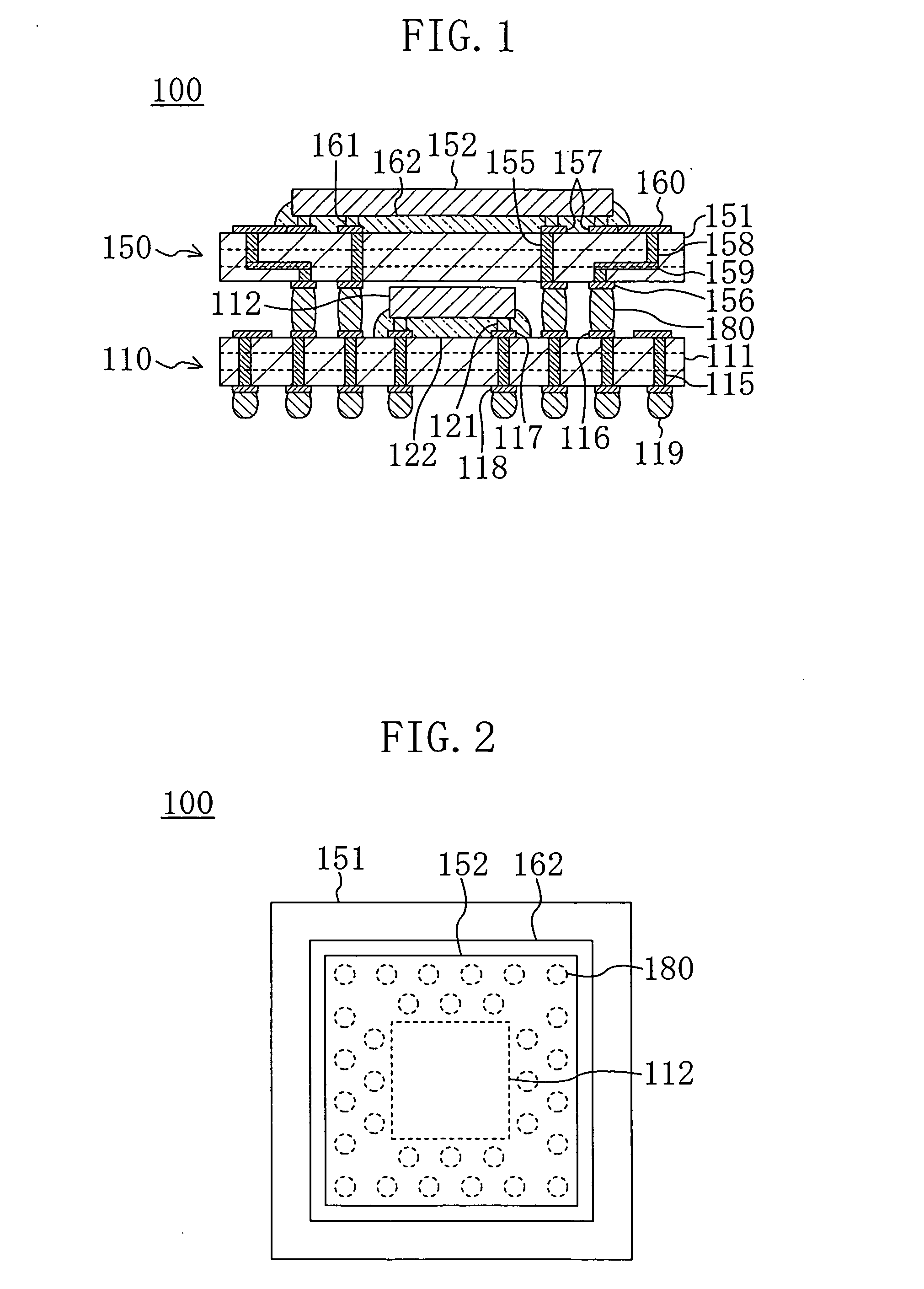
[0044]FIG. 1 shows a cross-sectional structure of a stacked semiconductor module 100 according to a first embodiment of the present invention, and FIG. 2 shows a plan structure of the stacked semiconductor module 100.

[0045] The stacked semiconductor module 100 is designed so that a second semiconductor device 150 with a second semiconductor chip 152 mounted to the top surface of a second semiconductor substrate 151 is stacked above a first semiconductor device 110 with a first semiconductor chip 112 mounted to a first semiconductor substrate 111.

[0046] In the first semiconductor substrate 111 having a multilayer interconnection structure, the center portion of the top surface thereof is provided with a region where the first semiconductor chip 112 is disposed. The inside of the first semiconductor substrate 111 is provided with a plurality of through conductors 115 extending from the top surface to the bottom surface. The top surface of the first semiconductor substrate 111 is pro...

second embodiment

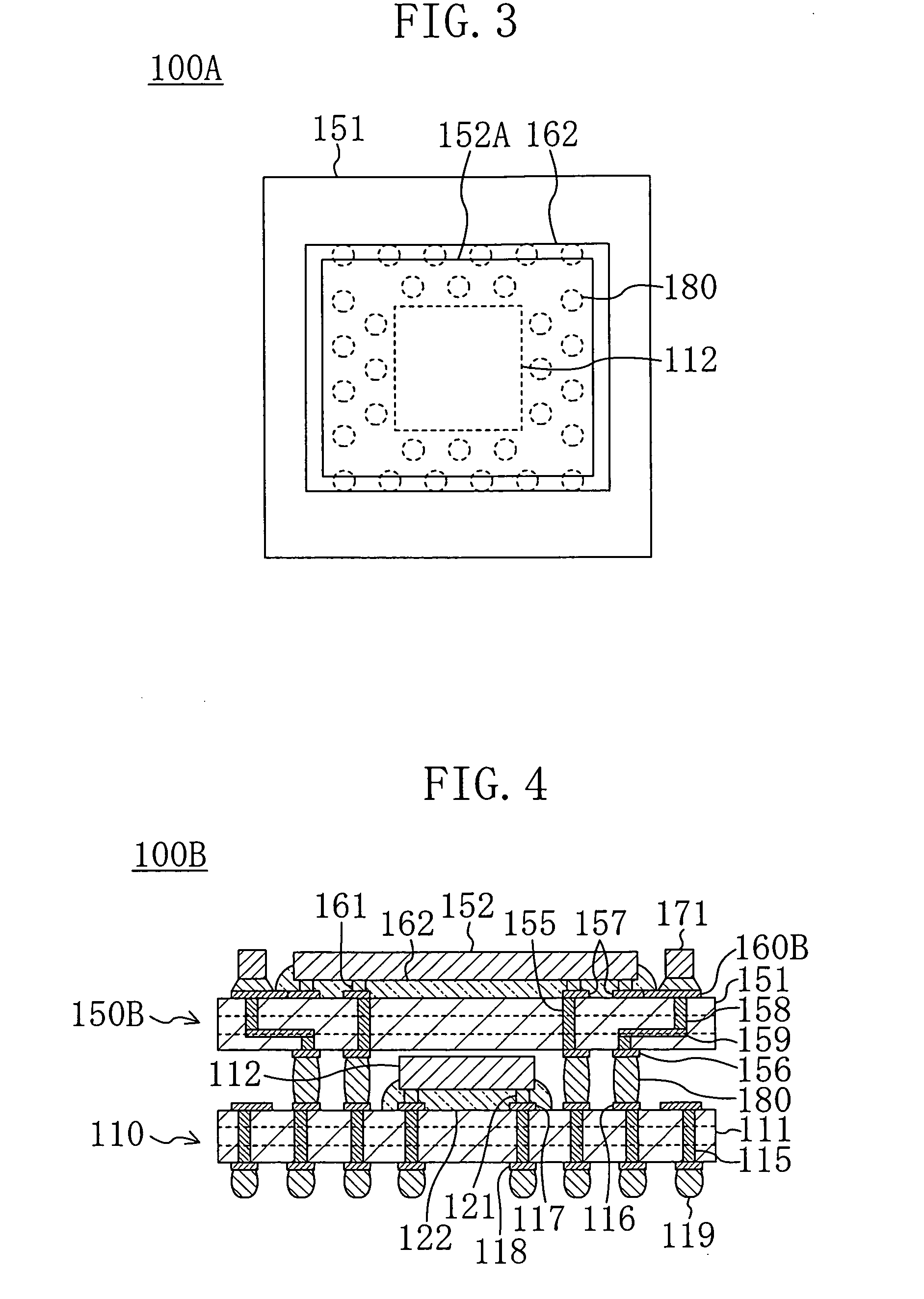
[0070]FIG. 5 shows a cross-sectional structure of a stacked semiconductor module 200 according to a second embodiment of the present invention, and FIG. 6 shows a plan structure of the stacked semiconductor module 200.

[0071] The stacked semiconductor module 200 is designed so that a second semiconductor device 250 with a second semiconductor chip 252 mounted to the top surface of a second semiconductor substrate 251 is stacked above a first semiconductor device 210 with a first semiconductor chip 212 mounted to a first semiconductor substrate 211. The second embodiment is characterized in that the second semiconductor chip 252 is composed of a plurality of semiconductor chips disposed on the same plane.

[0072] In the first semiconductor substrate 211 having a multilayer interconnection structure, the center portion of the top surface thereof is provided with a region where the first semiconductor chip 212 is disposed. The inside of the first semiconductor substrate 211 is provided ...

third embodiment

[0087]FIG. 8 shows a cross-sectional structure of a stacked semiconductor module 300 according to a third embodiment of the present invention.

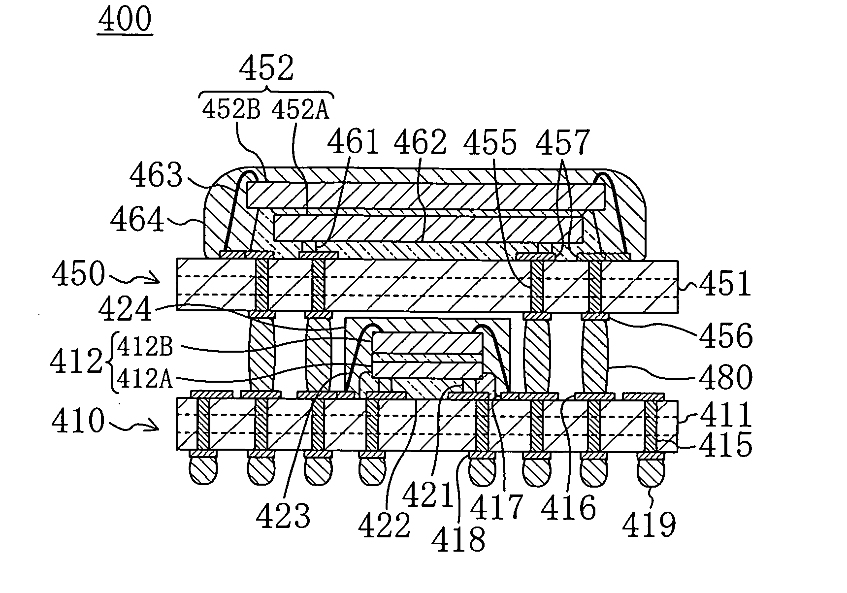
[0088] The stacked semiconductor module 300 is designed so that a second semiconductor device 350 with a second semiconductor chip 352 mounted to the top surface of a second semiconductor substrate 351 is stacked above a first semiconductor device 310 with a first semiconductor chip 312 mounted to the bottom surface of a first semiconductor substrate 311. The third embodiment is characterized in that the first semiconductor chip 312 is disposed below the bottom surface of the first semiconductor substrate 311.

[0089] In the first semiconductor substrate 311 having a multilayer interconnection structure, the center portion of the bottom surface thereof is provided with a region where the first semiconductor chip 312 is disposed. The inside of the first semiconductor substrate 311 is provided with a plurality of through conductors 315 extending...


PUM


Abstract

A stacked semiconductor module is made by stacking a second semiconductor device having a second semiconductor chip mounted to the top surface of a second semiconductor substrate above the top surface of a first semiconductor device having a first semiconductor chip mounted to a first semiconductor substrate. The top surface of the first semiconductor substrate is provided with a first connection terminal and the bottom surface of the first semiconductor substrate is provided with an external connection terminal. A region of the bottom surface of the second semiconductor substrate lying opposite to the second semiconductor chip is provided with a second connection terminal. A conductive connecting member connects the first connection terminal to the second connection terminal.

Description

CROSS-REFERENCE TO RELATED APPLICATIONS [0001] This application claims priority under 35 U.S.C. § 119 on Patent Application No. 2005-313186 filed in Japan on Oct. 27, 2005, the entire contents of which are hereby incorporated by reference. BACKGROUND OF THE INVENTION [0002] (a) Fields of the Invention [0003] The present invention relates to the structure of a stacked semiconductor module three-dimensionally constructed by stacking a second semiconductor device above a first semiconductor device. In particular, the present invention relates to the mount structure of the module. [0004] (b) Description of Related Art [0005] With a demand for size reduction and functionality enhancement of electronic equipment of various types including a cellular phone and a digital camera, attention is being given to a stacked semiconductor module which is made by stacking semiconductor devices each of which has electronic components, particularly, one or more semiconductor chips mounted to a semicond...

Claims


Application Information

Patent Timeline
Patent Type & Authority Applications(United States)
IPC IPC(8): H01L23/52
CPCH01L25/0652H01L2924/15321H01L25/105H01L2224/16225H01L2224/48225H01L2224/73204H01L2224/73265H01L2224/83102H01L2224/92125H01L2225/0651H01L2225/06517H01L2225/0652H01L2225/06558H01L2225/06572H01L2225/06582H01L2225/06596H01L2924/01078H01L2924/09701H01L2924/15184H01L2924/15311H01L2924/15331H01L2924/19041H01L2924/19105H01L2924/3011H01L2224/32145H01L2224/32225H01L2224/48227H01L2924/3511H01L25/0657H01L2224/16235H01L2225/1058H01L2225/1023H01L2924/00012H01L2924/00011H01L2924/00H01L24/73H01L23/12
Inventor KAWABATA, TAKESHIFUKUDA, TOSHIYUKI
Owner PANASONIC CORP
Why Eureka
Try Eureka