Semiconductor device and manufacturing method thereof

a technology of semiconductors and semiconductors, applied in the direction of semiconductor devices, electrical devices, transistors, etc., can solve the problems of inability to meet the requirements of a single insulating film, so as to prevent the tft from increasing the off current

Inactive Publication Date: 2007-05-10
SEMICON ENERGY LAB CO LTD
View PDF48 Cites 7 Cited by
  • Summary
  • Abstract
  • Description
  • Claims
  • Application Information

AI Technical Summary

Benefits of technology

[0016] The present invention has been made in view of the above, and an object of the present invention is therefore to provide a semiconductor device having a shielding film that is capable of preventing a TFT from increasing its OFF current because of incident light coming from the active matrix substrate side.
[0022] With the above structure, the surface of the insulating film can be leveled to avoid giving the TFT to be formed on the insulating film a poor characteristic. The polishing by CMP also helps to reduce the bending of the substrate which is caused by the stress of the insulating film, to a certain degree.
[0023] The shielding film can block light from the active matrix substrate side which otherwise would irradiate the channel formation region of the TFT, thereby preventing the light from increasing OFF current of the TFT. Being formed on the active matrix substrate side, the shielding film needs only a limited margin for positioning itself, thereby improving the aperture ratio.
[0024] The shielding film can be formed above the TFT and a wiring with an interlayer insulating film interposed between the shielding film and the TFT and the wiring, in addition to employing the structure of the present invention, namely, forming the shielding film between the active layer of the TFT and the substrate. Then light can more securely be prevented from entering the active layer, in particular, the channel formation region.
[0025] When the shielding film is formed between the active matrix substrate and the active layer of the TFT, the wiring may be formed simultaneously. If the same material is used for the wiring and the shielding film and if the wiring is a gate signal line or a source-signal line, image disturbance (discrimination) caused by orientation disorder in a liquid crystal material between pixels can be prevented.

Problems solved by technology

However, if the shielding film causes unevenness in the surface of the insulating film, the unevenness in turn deforms the active layer of the TFT and a characteristic of the TFT formed on the uneven insulating film is poor.
To be specific the mobility is undesirably increased.
Although the surface of the insulating film can be planar if the insulating film is sufficiently thick forming a thick insulating film takes time and it is no help in cutting the required time for the whole process of manufacturing the liquid crystal display.
Moreover, increased thickness is accompanied with increased risks of the substrate being bent and of the insulating film itself being peeled off the substrate due to the stress of the insulating film.

Method used


Image

  • Semiconductor device and manufacturing method thereof
  • Semiconductor device and manufacturing method thereof
  • Semiconductor device and manufacturing method thereof

Examples


embodiment 1

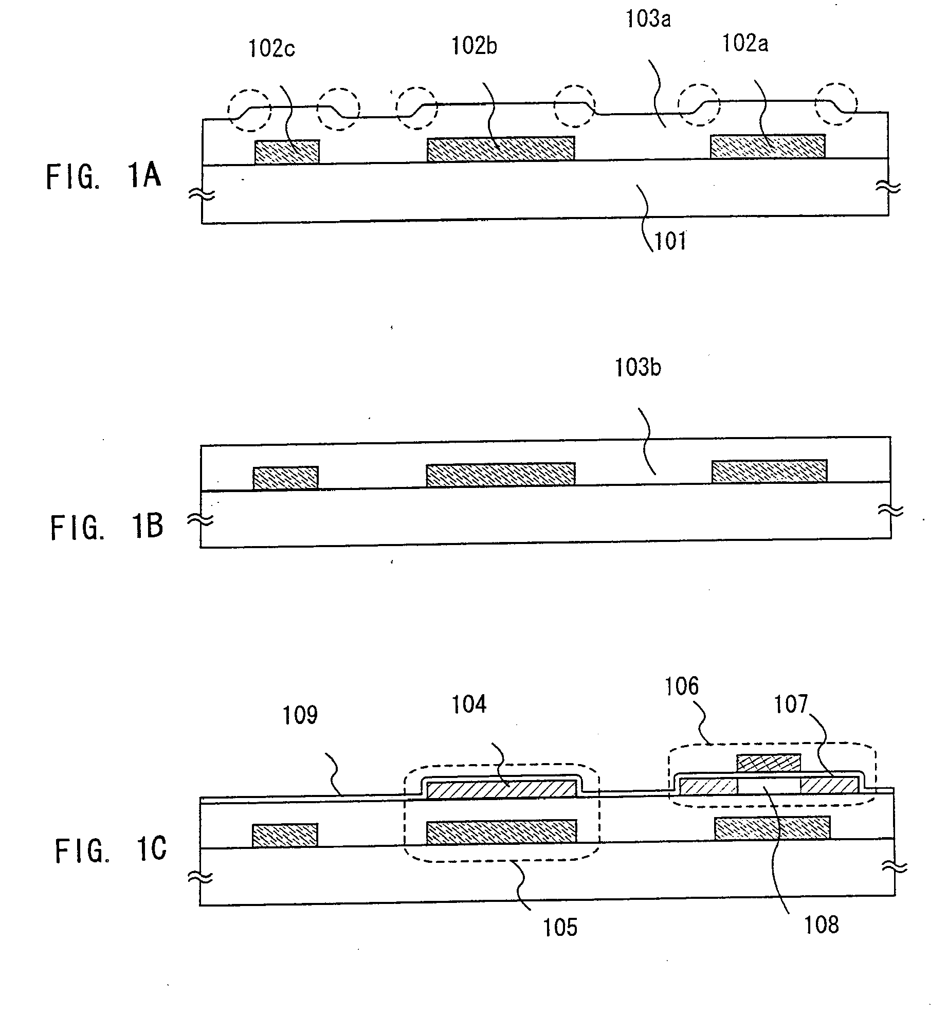
[0125] A top surface diagram of an example of a liquid crystal display with a light shielding film of the present invention is shown in FIG. 2.

[0126] Reference numeral 201 denotes a source signal line, and reference numeral 202 denotes a gate signal line. Reference numeral 203 is a lower layer capacitor wiring, and is provided in parallel with the gate signal line 202.

[0127] Reference numeral 205 denotes a pixel TFT, and controls input of the video signal which has been input to the source signal line 201 to the pixel electrode 208. The pixel TFT 205 has an active layer 206 and a gate electrode 207, and a channel forming region is provided in a region where the gate electrode 207 and the active layer 206 overlap. A light shielding film 204 is formed under the active layer 206, which overlaps with the entire channel forming region.

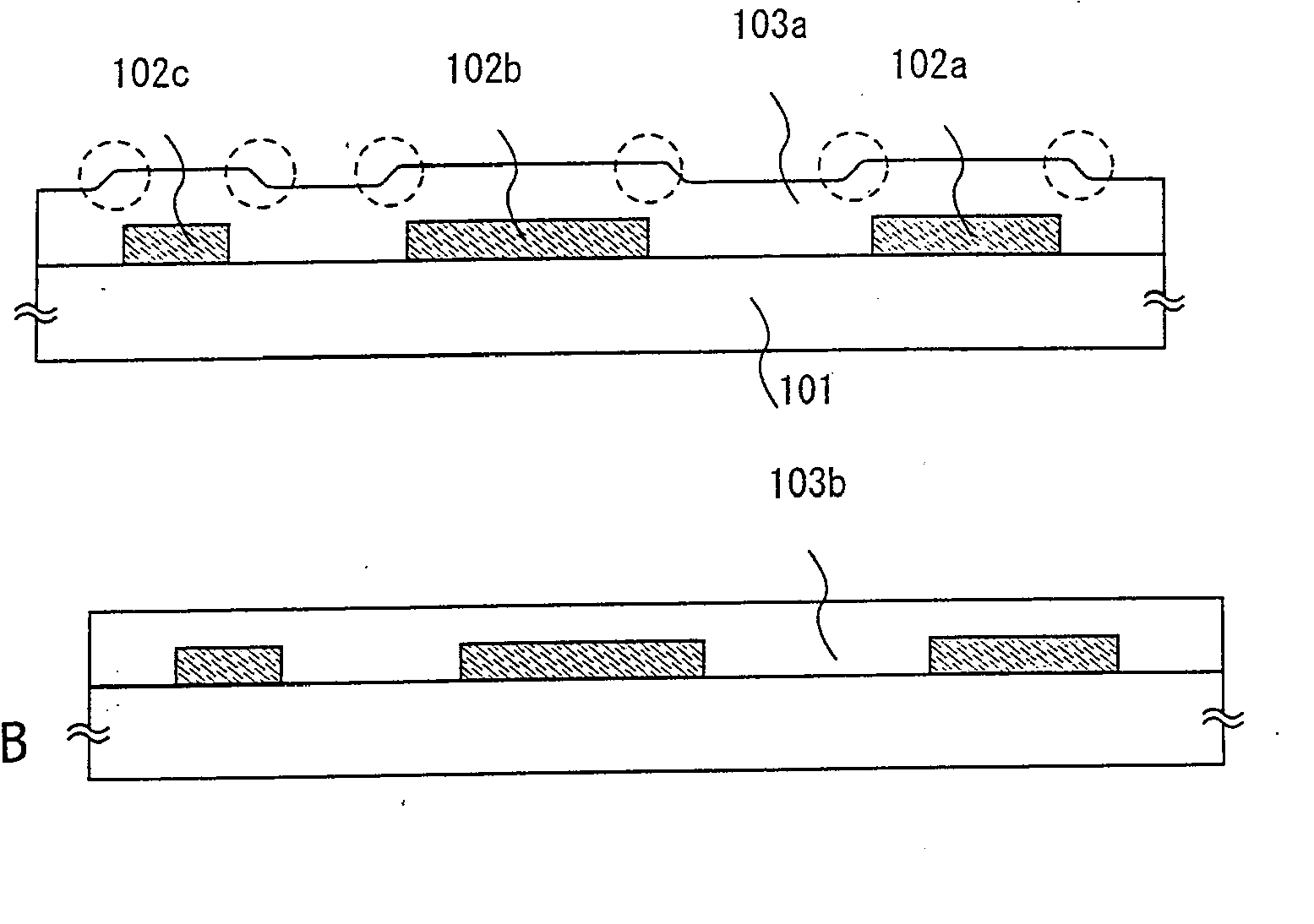
[0128] In this embodiment, the gate signal line 202 corresponds to the lower layer wiring 102c in FIG. 1. A planarization insulating film (not shown) is...

embodiment 2

[0133] In this embodiment, a detailed description will be given of a method of fabricating a pixel portion and TFTs (n-channel TFT and p-channel TFT) of a driver circuit provided in the periphery of the pixel portion on the same substrate at the same time.

[0134] First, as shown in FIG. 3A, a light shielding film 301a, a gate signal line 301b, and a lower layer capacitor wiring 301c are formed on an active matrix substrate (hereinafter, referred to as substrate) made of glass such as barium borosilicate glass or alumino borosilicate glass, typified by #7059 glass or #1737 glass of Corning Inc, or quartz.

[0135] Next, the light shielding film 301a, a gate signal line 301b, and a lower layer capacitor wiring 301c are formed simultaneously. Specifically, W is formed with a thickness of 0.1 μm to 0.5 μm (in this embodiment 0.3 μm), and thereafter an ICP (Inductively Coupled Plasma) etching method is used, in which CF4 and Cl2 are mixed in an etching gas, and an RF (13.56 MHz) power of 5...

embodiment 3

[0173] This embodiment gives a description of the structure of a CMP apparatus used in polishing by CMP.

[0174]FIG. 7A shows a side view of a CMP apparatus according to this embodiment and FIG. 7B shows a perspective view thereof. Reference symbol 701 denotes a platen, which is rotated by a driving shaft (a) 702 in the direction indicated by the arrow or in the opposite direction. The driving shaft (a) 702 is fixed by an arm (a) 703 to a fixed position.

[0175] A pad 704 is placed on the platen 701. The pad 704 may be a known polishing cloth or polishing pad. Slurry is supplied to the pad 704 from a slurry supplying nozzle 705. In this embodiment, the slurry is supplied from the slurry supplying nozzle 705 to a slurry supply position 710 that is placed substantially at the center of the pad 704. A known material can be used for the slurry.

[0176] Reference symbol 706 denotes a carrier having a function of rotating an active matrix substrate 707 on the pad 704 with the substrate fixed...


PUM


Abstract

OFF current of a TFT is reduced. There is provided a semiconductor device comprising: a substrate; a shielding film formed so as to be in contact with the substrate; a planarization insulating film formed on the substrate so as to cover the shielding film; and a semiconductor layer formed so as to be in contact with the planarization insulating film. The semiconductor device is characterized in that the shielding film overlaps the semiconductor layer with the planarization insulating film sandwiched therebetween, and that the planarization insulating film is polished by CMP before the semiconductor layer is formed.

Description

BACKGROUND OF THE INVENTION [0001] 1. Field of the Invention [0002] The present invention relates to a semiconductor device using a semiconductor element (an element that is formed of a semiconductor film), particularly, to a liquid crystal display. The present invention also relates to electronic equipment employing the liquid crystal display for a display unit. [0003] 2. Description of Related Art [0004] A technique that has been attracting attention in recent years is to fabricate a thin film transistor (TFT) using a semiconductor film (with a thickness on the order of several nm to several hundreds nm) that is formed on a substrate having an insulating surface. The thin film transistor is applied to a wide range of electronic devices, including ICs and semiconductor devices. Its application to a switching element for a liquid crystal display is especially desired to be developed swiftly. [0005] An active matrix liquid crystal display has a pixel portion comprising a plurality of...

Claims


Application Information

Patent Timeline
Patent Type & Authority Applications(United States)
IPC IPC(8): H01L31/12H01L27/15H01L33/00H01L29/16H01L21/336H01L21/77H01L21/84H01L27/12H01L29/423H01L29/49H01L29/786
CPCH01L27/12H01L29/42384H01L29/4908H01L29/66757H01L27/1248H01L29/78624H01L29/78633H01L29/78636H01L2029/7863H01L29/78621H01L29/786
Inventor YAMAZAKI, SHUNPEIKOYAMA, JUN
Owner SEMICON ENERGY LAB CO LTD
Why Eureka
Try Eureka