Socket base adaptable to a load board for testing IC

Inactive Publication Date: 2007-05-10
SILICON INTEGRATED SYSTEMS
View PDF8 Cites 14 Cited by
  • Summary
  • Abstract
  • Description
  • Claims
  • Application Information

AI Technical Summary

Benefits of technology

[0010] In view of the foregoing, it is an object of the present invention to provide a detachable and combinable socket base to simplify the replacement procedure of the probe element.
[0011] According to the object, the present invention provides a socket base adaptable to a load board for testing semiconductor devices. The socket base includes a first fixing element having an opening, first guide structures, and coupling plates; a second fixing element having first coupling structures, second guide structures; and a probe element having fixing pin holes. The first fixing element and the second fixing element are detachable and combinable by using the coupling plates. Accordingly, the procedure for replacing the probe element is simplified, consumed time is reduced, and efficiency is therefore increased.

Problems solved by technology

One of the difficulties concerning the probe element in the conventional test equipment is the complex or time-consuming procedure to install or replace the probe element.

Method used


Image

  • Socket base adaptable to a load board for testing IC
  • Socket base adaptable to a load board for testing IC
  • Socket base adaptable to a load board for testing IC

Examples


Embodiment Construction

[0019] The detailed description of the present invention will be discussed in the following embodiments, which are not intended to limit the scope of the present invention, but can be adapted for other applications. While drawings are illustrated in details, it is appreciated that the quantity of the disclosed components may be greater or less than that disclosed, except expressly restricting the amount of the components.

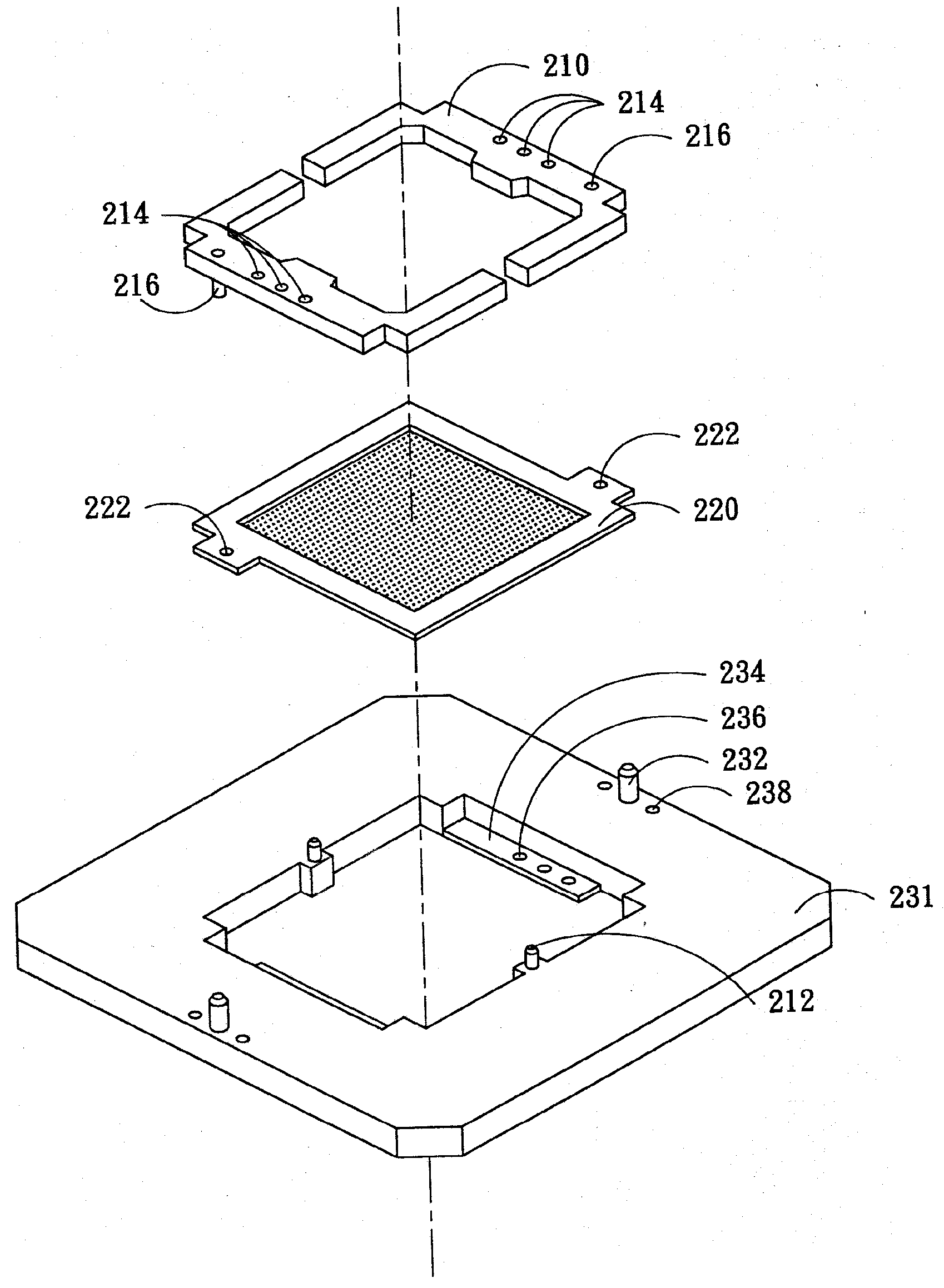
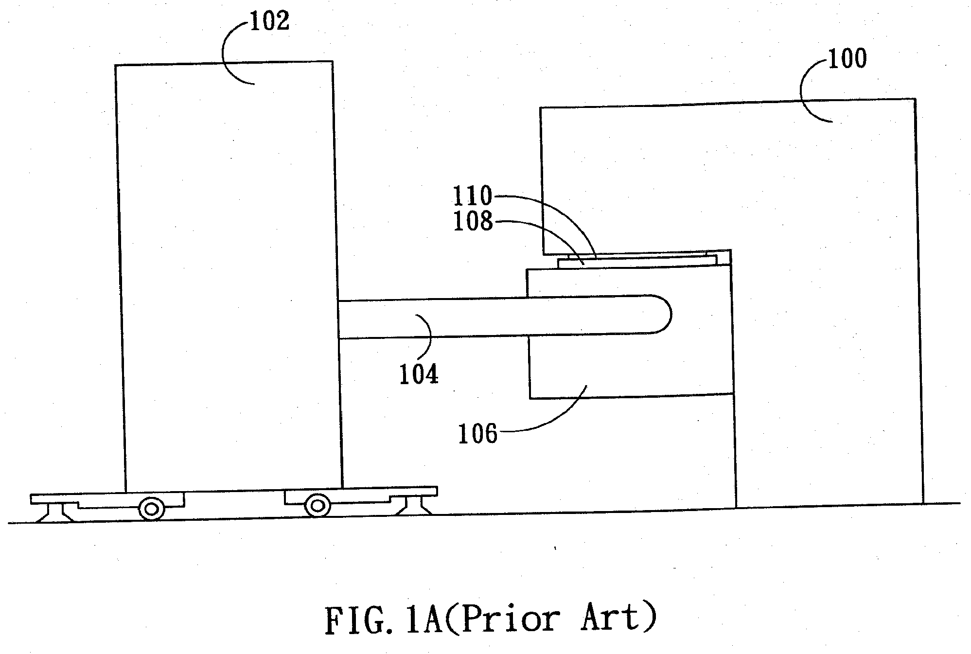
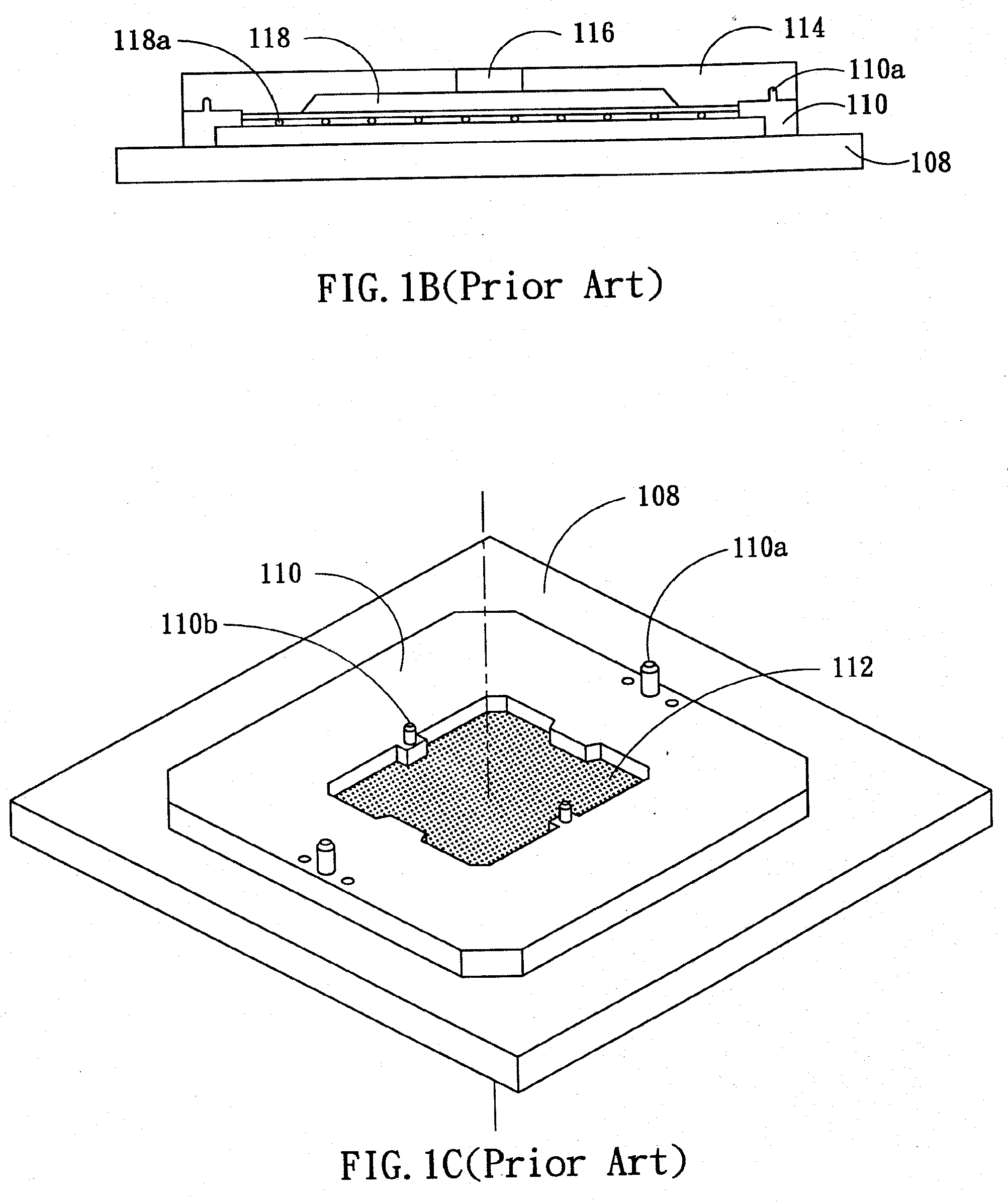
[0020]FIG. 2 schematically shows the composing elements of a socket base according to one embodiment of the present invention. A first fixing element 230 has an opening in the middle thereof, two first guide pins 232 acting as the first guide structures, and a coupling plate 234. A second fixing element 210 is used to secure a probe element 220, which is a surface mount matrix (SMM) 220 in this embodiment. On a first side (that is, the top side in the figure) of the second fixing element 210 are some second guide pins 212 acting as the second guide structures, and ...


PUM


Abstract

A socket base adaptable to a load board for testing semiconductor devices is disclosed. The socket base includes a first fixing element having coupling plates, a probe element, and a second fixing element, which are detachable and combinable. Accordingly, the procedure for replacing the probe element is simplified, time is reduced, and efficiency is increased.

Description

FIELD OF THE INVENTION [0001] The present invention generally relates to a socket base adaptable for a load board, and more particularly to a detachable and combinable socket base for testing semiconductor devices. DESCRIPTION OF THE PRIOR ART [0002] The advancement of the integrated circuits manufacturing technique brings abundant electronic products to our modern life. In addition to attaining more compact electronic products, diverse integrated circuits are simultaneously applied into a single product to obtain more functions. In order to accomplish this goal, the quality of each integrated circuit is predominantly important. [0003] The manufacture of the integrated circuits passes through a series of strictly controlled steps. The circuit is firstly designed and applied to the manufacture of wafers, followed by cutting each manufactured wafer into chips. The chips are packaged and then tested to their functionality and reliability. The test is a critical step in which malfunctio...

Claims


Application Information

Patent Timeline
IPC IPC(8): G01R31/02
CPCG01R1/0483
Inventor TSAI, SHOU-NANLIAO, MU-SHENG
Owner SILICON INTEGRATED SYSTEMS
Why Eureka
Try Eureka