Liquid crystal display device

a liquid crystal display and display device technology, applied in the direction of thin material processing, instruments, chemistry apparatus and processes, etc., can solve the problems of reducing the effect, easy to disturb alignment, and long response time of the liquid crystal display device, and achieve excellent viewing angle characteristics and high brightness

Active Publication Date: 2007-05-10
SHARP KK
View PDF8 Cites 54 Cited by
  • Summary
  • Abstract
  • Description
  • Claims
  • Application Information

AI Technical Summary

Benefits of technology

[0013] An object of the invention is to provide a liquid crystal display device which can attain an excellent viewing angle characteristic and high brightness.
[0020] According to the invention, a liquid crystal display device can be implemented which can obtain an excellent viewing angle characteristic and high brightness.

Problems solved by technology

However, since the micro slit 116d has weaker alignment control than that of the linear protrusion and the main slit, the liquid crystal display device has a long response time of the liquid crystals, and the alignment is easily disturbed by a finger press or so.
In addition, the shift of the alignment orientation of liquid crystals also affects the viewing angle characteristic to reduce the effect that improves the white patch described above as well.
On this account, a problem arises that the light transmittance of a pixel is further decreased.

Method used


Image

  • Liquid crystal display device
  • Liquid crystal display device
  • Liquid crystal display device

Examples


first embodiment

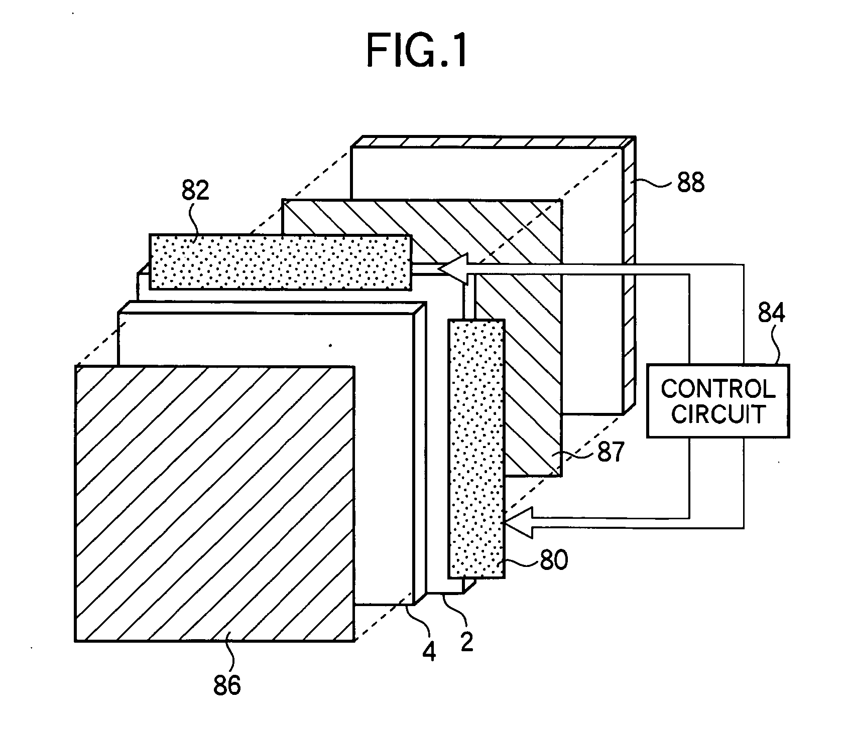
[0059] A liquid crystal display device according to a first embodiment of the invention will be described with reference to FIGS. 1 to 8. FIG. 1 shows the schematic configuration of the liquid crystal display device according to this embodiment. As shown in FIG. 1, the liquid crystal display device has a TFT substrate 2 provided with a gate bus line and a drain bus line which are formed as they intersect with each other through an insulating film, and a TFT (switching element) and a pixel electrode which are formed at every pixel. In addition, the liquid crystal display device has a opposite substrate 4 on which a color filter (CF) and a common electrode are formed, and which is disposed facing the TFT substrate 2. Between the substrates 2 and 4, liquid crystals 6 are sealed (not shown in FIG. 1).

[0060] To the TFT substrate 2, drive circuits are connected: a gate bus line drive circuit 80 on which a driver IC is mounted to drive a plurality of the gate bus lines, and a drain bus li...

example 1-1

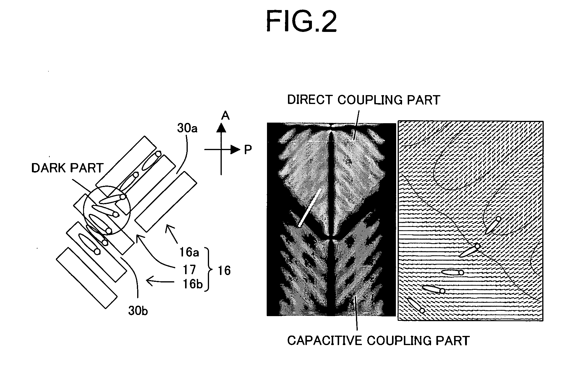
[0066]FIG. 4 shows the single pixel configuration of a liquid crystal display device according to the example 1-1 of the embodiment. As shown in FIG. 4, a pixel area is defined by a gate bus line 12 and a drain bus line 14 which intersect with each other through an insulating film. In the example, a direct coupling part 16a is disposed at the center of the pixel area, and a capacitive coupling part 16b is disposed at the upper part and the lower part in the pixel area as they sandwich the direct coupling part 16a in the drawing. The direct coupling part 16a is electrically connected to a source electrode of a TFT 20 through a contact hole and a control capacitance electrode 25. The capacitive coupling part 16b forms capacitance with the control capacitance electrode 25 which has the same potential as that of the source electrode of the TFT 20. In the example, alignment irregularities are basically small in a space 17 between the direct coupling part 16a and the capacitive coupling p...

example 1-2

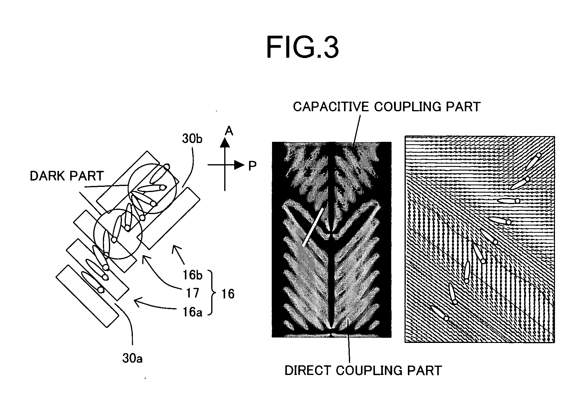
[0067]FIG. 5A shows the single pixel configuration of a liquid crystal display device according to the example 1-2 of the embodiment, and FIG. 5B shows the layout of a storage capacitor bus line 18, a storage capacitor electrode 19 and a control capacitance electrode 25 in that pixel. FIG. 6 shows the simulation result of the display state of a pixel in the liquid crystal display device according to the embodiment. In the example 1-1 above, the pixel area is split into three parts, a single direct coupling part 16a and two capacitive coupling parts 16b. Therefore, five alignment split lines exist vertically including the space 17. Since these parts become the dark lines, a fewer number of alignment split lines is preferable. As shown in FIGS. 5A, 5B and 6, in the example, a direct coupling part 16a is disposed in the upper pixel area, and a capacitive coupling part 16b is disposed in the lower pixel area. The pixel area was split into two parts to reduce the number of the alignment ...


PUM

PropertyMeasurementUnit
angleaaaaaaaaaa
widthaaaaaaaaaa
widthaaaaaaaaaa

Abstract

The invention has an object to provide a liquid crystal display device of an excellent viewing angle characteristic and high brightness, including: sandwiching liquid crystals containing polymerizable monomers between a first substrate with a pixel electrode having a micro slit and a second substrate facing the first substrate; polymerizing the monomers with voltage applied to the liquid crystals; and controlling an alignment orientation of the liquid crystals to a direction of extending the micro slit, wherein the pixel electrode includes: a direct coupling part electrically connected to a switching element; a capacitive coupling part electrically insulated from the switching element, and forming capacitance with a control capacitance electrode having a same potential as that of a source electrode of the switching element; and a space between the direct and capacitive coupling parts, wherein directions of extending the micro slit in the adjacent direct and capacitive coupling parts are orthogonal to each other.

Description

BACKGROUND OF THE INVENTION [0001] 1. Field of the Invention [0002] The present invention relates to a liquid crystal display device for use in a display unit of electronic appliances. [0003] 2. Description of the Related Art [0004] For a liquid crystal display device which can attain a wide viewing angle, a liquid crystal display device in MVA (Multi-domain Vertical Alignment) mode is known. The liquid crystal display device in the MVA mode has liquid crystals of negative dielectric anisotropy which are sealed between a pair of substrates, a vertical alignment film which aligns liquid crystal molecules almost vertically with respect to the substrate surface, and an alignment regulating structure which regulates the alignment orientation of liquid crystal molecules. For the alignment regulating structure, a linear protrusion formed of a dielectric and an open part (main slit) of an electrode are used. When voltage is applied, the liquid crystal molecules are tilted in the direction ...

Claims


Application Information

Patent Timeline
Patent Type & Authority Applications(United States)
IPC IPC(8): G02F1/1343C09K19/00
CPCC09K19/38C09K2019/0448G02F1/133707G02F1/133711Y10T428/10G02F2001/134354G02F2001/13775G02F1/13439Y10T428/1036G02F1/1393C09K2323/03C09K2323/00G02F1/134354G02F1/13775
Inventor HANAOKA, KAZUTAKAOHMURO, KATSUFUMITASHIRO, KUNIHIROHIROSAWA, JINSUGIURA, NORIOKANII, KENGOMAKIMOTO, SHOTAOHNO, YASUHIROTSUSHIMA, ISAOTANOSE, TOMONORITAKAGI, TAKASHIFUJIKAWA, TETSUYASASAKI, TAKAHIRO
Owner SHARP KK
Why Eureka
Try Eureka