Organic light emitting display device

a light-emitting display and organic technology, applied in the direction of organic semiconductor devices, electroluminescent light sources, thermoelectric devices, etc., can solve the problems of deteriorating image and dark pixels to be displayed, and achieve the effect of preventing a reduction in the aperture ratio

Active Publication Date: 2007-05-17
SAMSUNG DISPLAY CO LTD
View PDF23 Cites 39 Cited by
  • Summary
  • Abstract
  • Description
  • Claims
  • Application Information

AI Technical Summary

Benefits of technology

[0030] In addition, the organic light emitting display device of the present invention can prevent a reduction in an aperture ratio in compari

Problems solved by technology

Due to patterning flaws and external pressure, the anode electrode and the cathode electrode that are to be insulated from eac

Method used


Image

  • Organic light emitting display device
  • Organic light emitting display device
  • Organic light emitting display device

Examples


Embodiment Construction

[0041]FIG. 5A is a plan view of a unit pixel 500 according to an embodiment of the present invention. The unit pixel 500 is shown to include three sub-pixels 501, 502, 503. A first sub-pixel 501 has an organic emission layer whose thickness is thinner than that of any other sub-pixel. The first sub-pixel 501 includes two drive transistors M2, M3, and two first electrodes a1 and a2. The first sub-pixel 501 is, therefore, a divided sub-pixel. Each of other sub-pixels 502, 503 includes one drive transistor and a first electrode.

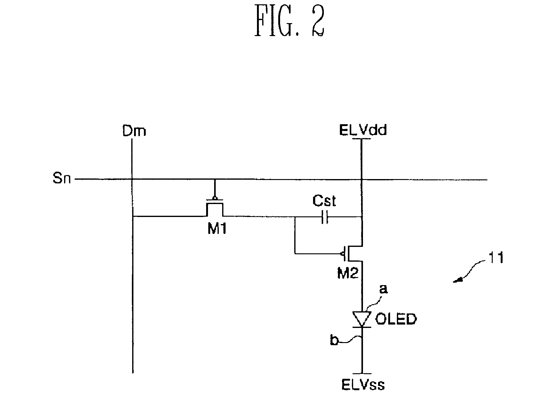
[0042]FIG. 5B is a circuit diagram showing a sub-pixel having a thin organic emission layer according to an embodiment of the present invention. The sub-pixel shown is a divided sub-pixel included in a representative pixel among n×m pixels, and is connected to a data line Dm and a scan line Sn.

[0043] The circuit for the divided sub-pixel includes a switching transistor M1, a first drive transistor M2, a second drive transistor M3, a capacitor Cst, and an organ...


PUM


Abstract

An organic light emitting display device, which may maximize aperture ratio of a pixel while also reducing the perception of a dark spot when a sub-pixel is partially short-circuited. The organic light emitting display device includes a plurality of pixels having sub-pixels. Some of the sub-pixels may have a thin organic emission layer which makes them likely to short-circuit across the thin organic emission layer. These sub-pixels are formed as divided sub-pixels including at least two drive transistors and operate such that even if one part of the divided sub-pixel has a short circuit, the other part will continue to emit light. Accordingly, while luminance is reduced as a result of short circuiting, a completely dark spot will not appear in the place of the pixel including the short circuit.

Description

CROSS-REFERENCE TO RELATED APPLICATIONS [0001] This application claims priority to and the benefit of Korean Patent Application No. 10-2005-0108795, filed on Nov. 14, 2005, in the Korean Intellectual Property Office, the entire content of which is incorporated herein by reference. BACKGROUND [0002] 1. Field of the Invention [0003] The present invention relates to an organic light emitting display device, and more particularly to an organic light emitting display device decreasing the perception of a dark pixel occurring due to a short-circuit between a first electrode and a second electrode of an organic light emitting diode. [0004] 2. Discussion of Related Art [0005] Organic light emitting display devices are spontaneous emission devices that emit light by re-combination of electrons supplied from a cathode and holes supplied from an anode. An electroluminescent (EL) display using the organic light emitting display device does not require additional back light, has a wider angle of...

Claims


Application Information

Patent Timeline
IPC IPC(8): H01L29/08
CPCH01L27/3202H01L27/3211H01L27/3244H01L2251/558H10K59/84H10K59/35H10K59/12H10K2102/351H05B33/02
Inventor KIM, EUN AH
Owner SAMSUNG DISPLAY CO LTD
Why Eureka
Try Eureka