Display device including a trench and manufacturing method thereof

a technology of a display device and a manufacturing method, which is applied in the field of display devices and their manufacturing methods, can solve the problems of difficult to form electrodes in patterns, and achieve the effects of reducing process costs, high etching resistance, and simplifying manufacturing processes

Active Publication Date: 2021-12-14
LG DISPLAY CO LTD
View PDF7 Cites 0 Cited by
  • Summary
  • Abstract
  • Description
  • Claims
  • Application Information

AI Technical Summary

Benefits of technology

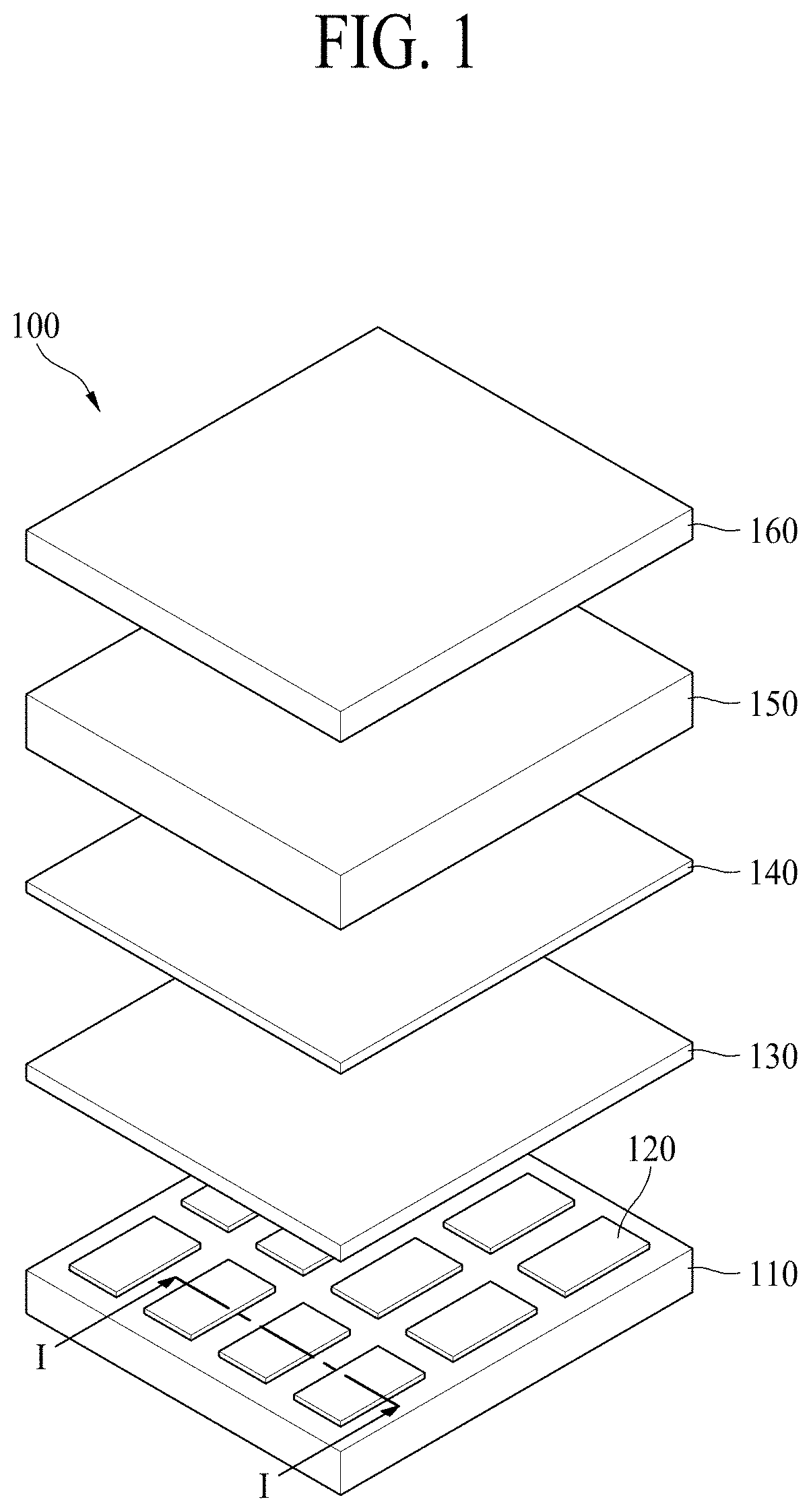
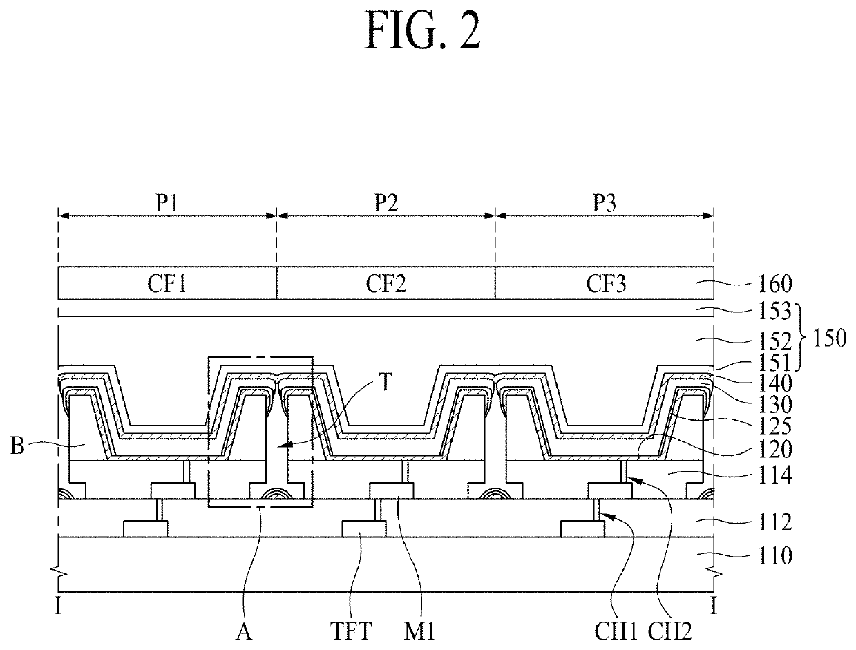
[0009]According to the present disclosure, a first electrode and a light emitting layer may be self-aligned by trenches and may be formed by pixels. Accordingly, because the first electrode may be formed without using a particular mask, it is possible to simplify manufacturing processes and reduce process costs. Because the first electrode may be formed without performing any particular etching process, the first electrode can also be formed of a metal material having high etching resistance such as silver (Ag).
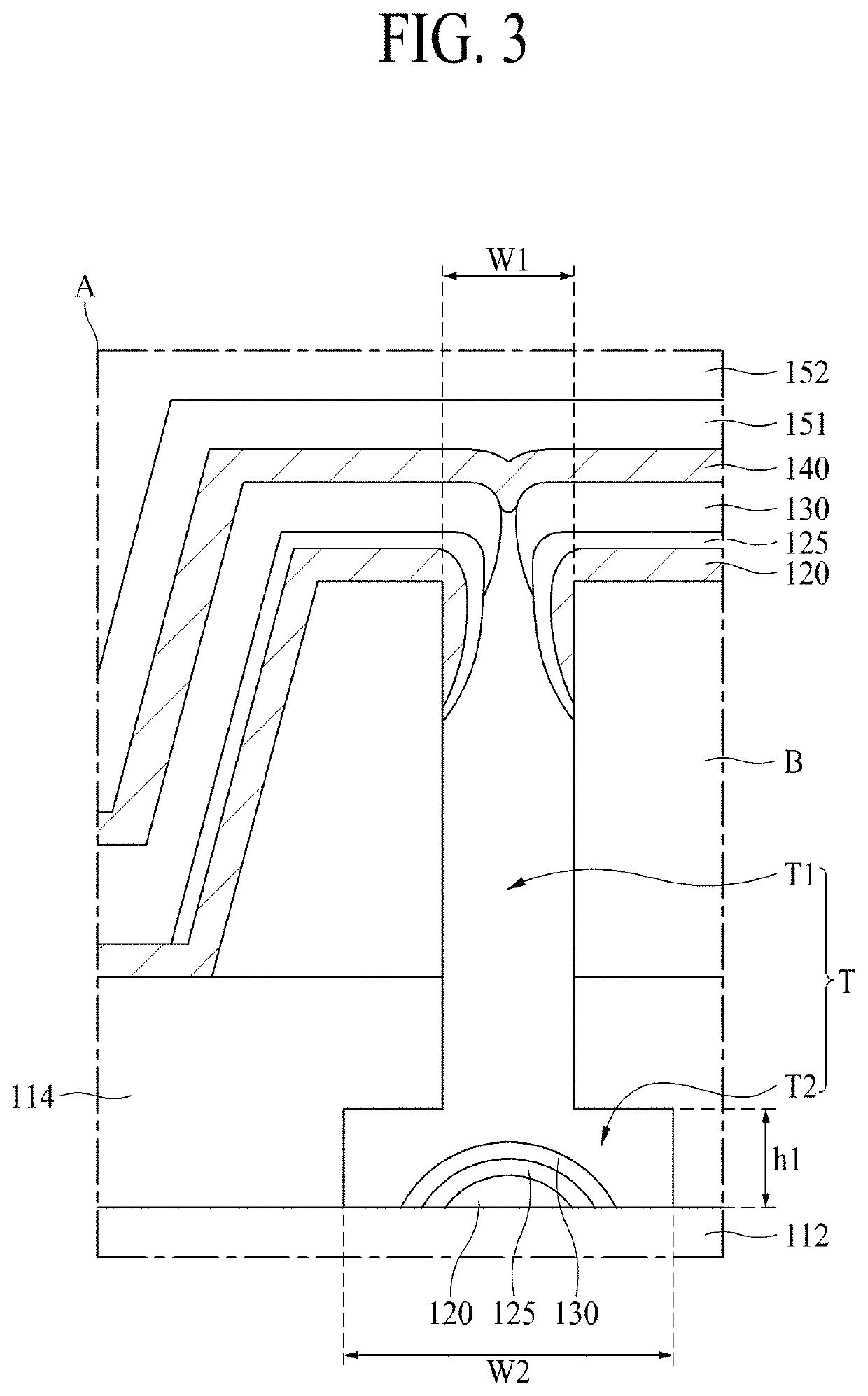
[0010]Because the first electrode may also be formed on the side surface of the bank, light propagating to the bank can be reflected upward. Accordingly, it is possible to reduce loss of light that is emitted from the light emitting layer. Because the light emitting layer may be cut off in a trench, it is possible to minimize or reduce an influence of a leakage current from the light emitting layer on a neighboring pixel. Because the bank may be formed after the trench has been formed, it is possible to minimize or reduce the top area of the bank. Accordingly, it is possible to maximize an aperture ratio of a pixel.

Problems solved by technology

However, in such a head-mounted display with an ultrahigh definition, there is a problem in that it is difficult to form electrodes included in pixels in patterns due to minute pixel pitches.

Method used


Image

  • Display device including a trench and manufacturing method thereof
  • Display device including a trench and manufacturing method thereof
  • Display device including a trench and manufacturing method thereof

Examples


Embodiment Construction

[0022]Reference will now be made in detail to the example embodiments of the present disclosure, examples of which may be illustrated in the accompanying drawings. Wherever possible, the same reference numbers will be used throughout the drawings to refer to the same or like parts. Advantages and features of the present disclosure, and implementation methods thereof will be clarified through following example embodiments described with reference to the accompanying drawings. The present disclosure may, however, be embodied in different forms and should not be construed as limited to the example embodiments set forth herein. Rather, these example embodiments are provided so that this disclosure will be thorough and complete, and will fully convey the scope of the present disclosure to those skilled in the art.

[0023]A shape, a size, a ratio, an angle, and a number disclosed in the drawings for describing example embodiments of the present disclosure are merely examples, thus the prese...


PUM

PropertyMeasurementUnit
widthaaaaaaaaaa
weightaaaaaaaaaa
thicknessaaaaaaaaaa

Abstract

A display device includes: a substrate; a plurality of pixels on the substrate; an insulating film on the substrate; a bank on the insulating film, wherein the bank partitions the plurality of pixels; a first trench in the bank; and a second trench in the insulating film. A method of manufacturing a display device includes: forming a first lower metal layer and a second metal layer in patterns on a substrate; forming a first insulating film on the first lower metal layer and the second lower metal layer; forming a second insulating film on the first insulating film; forming a first trench to expose the second lower metal layer by performing a first etching process; and forming a second trench by performing a second etching process to etch the second lower metal layer exposed from a bottom of the first trench.

Description

[0001]This application claims the benefit of and priority to Korean Patent Application No. 10-2018-0089440, filed on Jul. 31, 2018, which is hereby incorporated by reference in its entirety as if fully set forth herein.BACKGROUNDTechnical Field[0002]The present disclosure relates to a display device and manufacturing method thereof, and more particularly, to a display device in which electrodes can be easily formed and a manufacturing method thereof.Discussion of the Related Art[0003]With advancement in information-oriented societies, requirements for display devices that display an image have increased in various types. Recently, various display devices such as a liquid crystal display (LCD) device, plasma display panel (PDP) device, and organic light emitting display (OLED) device have been widely utilized. An OLED device is of a spontaneous emission type. An OLED device also has a viewing angle and a contrast ratio that are more desirable than those of an LCD. An OLED may also ha...

Claims


Application Information

Patent Timeline
Patent Type & Authority Patents(United States)
IPC IPC(8): H01L27/32H01L51/56G02B27/01G06F1/16
CPCH01L27/3246H01L27/3258H01L27/3276H01L51/56G02B27/0172G06F1/163H01L27/322H01L2227/323H10K59/123H10K59/124H10K59/122H10K50/813H10K50/818H10K71/00H10K59/38H10K50/80H10K59/131H10K59/1201
Inventor LIM, HYEONG-JUNYOON, DOO-HYNPARK, HAN-SUN
Owner LG DISPLAY CO LTD
Why Eureka
Try Eureka