Method for removing photoresist

a technology of photoresist and stripping, which is applied in the field of stripping a photoresist, can solve the problems of low yield in semiconductor production, poor corrosion resistance of low-k materials, and a single layer of wiring circuits, and achieve good corrosion resistance

Inactive Publication Date: 2005-08-11
TOKYO OHKA KOGYO CO LTD
View PDF3 Cites 94 Cited by
  • Summary
  • Abstract
  • Description
  • Claims
  • Application Information

AI Technical Summary

Benefits of technology

[0015] The present invention has been made in consideration of the above-mentioned situation, and its object is to provide a method for stripping a photoresist which, even when employed in a process with no O2 plasma ashing treatment for micropatterning a substrate that has at least copper (Cu) wiring and a low-dielectric layer thereon, enables effective stripping of an etched photoresist film and an etching residue and which exhibits good corrosion resistance not having any negative influence on the dielectric constant of the low-dielectric layer.

Problems solved by technology

It is a trend in recent years that wiring circuits are becoming minute and multilayered as integration degree of semiconductor devices increases and chip size reduces, in which there arise problems in semiconductor devices, i.e., resistance of metallic layers (wiring resistance) and wiring delay caused by wiring capacities.
If these deposits are not completely removed, then it causes a problem in that the yield in semiconductor production may lower.
It is said that the material of the type having such a low dielectric constant (low-k material) is poorly resistant to ashing or is not resistant to ashing, and when such a low-k material is used, a process not including an O2 plasma ashing step after etching must be employed.

Method used


Image

  • Method for removing photoresist
  • Method for removing photoresist
  • Method for removing photoresist

Examples


examples

[0069] The invention is described in more detail with reference to the following Examples, to which, however, the invention should not be limited. Unless otherwise specifically indicated, the amount is in terms of % by mass.

examples 1 to 6

[0070] A substrate having a Cu wiring thereon that is overlaid with an SiOC layer (carbon-doped oxide layer; low-k layer) was used. A positive photoresist, TDUR-P722 (by Tokyo Ohka Kogyo Co., Ltd.) was coated on the substrate, and heated at 140° C. for 90 seconds to form a photoresist layer, and then selectively exposed to light using S-203B (by Nikon Corp.), then further heated at 140° C. for 90 seconds (post-exposure baking treatment), and developed with an aqueous 2.38 mas. % tetraammonium hydroxide (TMAH) solution to form a photoresist pattern. Next, the SiOC layer was etched.

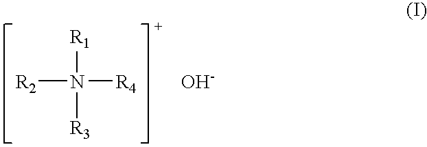
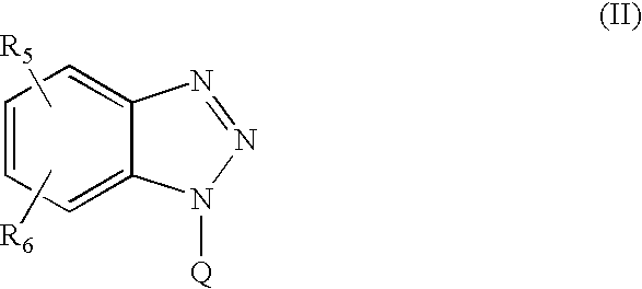
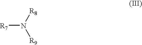
[0071] After thusly etched, the substrate was contacted with ozone water for 15 minutes. The ozone water had been prepared by bubbling ozone gas into pure water for 15 minutes. Subsequently, the substrate was dipped (at 60° C. for 30 seconds) in a photoresist stripping solution having the composition as in Table 1 below (stripping solutions A to F).

[0072] The surface of the thusly treated substrate was ob...

examples 7 to 12

[0073] The substrate that had been etched in the same manner as in Examples 1 to 6 was contacted with aqueous 30 mas. % hydrogen peroxide heated at 60° C., for 30 minutes, and then dipped (at 60° C. for 30 seconds) in a photoresist stripping solution having the composition as in Table 1 below (stripping solutions A to F).

[0074] The surface of the thusly treated substrate was observed with SEM (scanning electronic microscope), and it was found that the photoresist pattern and the etching residues had been completely removed. No corrosion was observed on the low-dielectric layer.


PUM

PropertyMeasurementUnit
dielectric constantaaaaaaaaaa
temperatureaaaaaaaaaa
water-solubleaaaaaaaaaa

Abstract

Disclosed is a method for stripping a photoresist comprising: (I) providing a photoresist pattern on a substrate where the substrate has at least a copper (Cu) wiring and a low-dielectric layer thereon, and selectively etching the low-dielectric layer by using the photoresist pattern as a mask; (II) contacting the substrate after the step (I), with ozone water and/or aqueous hydrogen peroxide; and (III) contacting the substrate after the step (II), with a photoresist stripping solution that contains at least a quaternary ammonium hydroxide. The present invention provides a method for stripping a photoresist that enables to strip effectively photoresist films and etching residues after etching step even in a process not including an O2 plasma ashing treatment in micropatterning of a substrate having at least Cu wiring and a low-dielectric layer thereon, as in a dual damascene forming process, and, in addition, the method of the invention does not have any negative influence on the dielectric constant of the low-dielectric layer, and ensures an excellent anti-corrosivity.

Description

TECHNICAL FIELD [0001] The present invention relates to a method for stripping a photoresist formed on a substrate having at least a copper (Cu) wiring and a low-dielectric layer thereon. In particular, the invention is favorably applied to a method for stripping a photoresist in a process not including a conventional O2 plasma ashing step in the fabrication of semiconductor devices, such as ICs and LSIs. BACKGROUND ART [0002] Semiconductor devices, such as IC and LSIs, are produced in the following process. A photoresist is uniformly coated on an electroconductive metallic layer, an insulating layer and a low-dielectric material layer formed on a substrate, such as a silicon wafer, by CVD vapor deposition process or the like. The photoresist is selectively subjected to exposure and development to form a photoresist pattern. The electroconductive metallic layer, the insulating layer and the low-dielectric material layer formed by CVD vapor deposition are selectively etched by using ...

Claims


Application Information

Patent Timeline
Patent Type & Authority Applications(United States)
IPC IPC(8): G03F7/42H01L21/027H01L21/304
CPCG03F7/425G03F7/42
Inventor YOKOI, SHIGERUWAKIYA, KAZUMASAHARAGUCHI, TAKAYUKI
Owner TOKYO OHKA KOGYO CO LTD
Why Eureka
Try Eureka