Semiconductor storage device equipped with ECC function

a technology of semiconductor storage device and function, which is applied in the direction of digital storage, error detection/correction, instruments, etc., can solve the problem that the technology cannot deal with the part writing, and achieve the effect of increasing the operation speed of the semiconductor storage device, reducing the time for data write processing, and increasing the speed of data write processing

Inactive Publication Date: 2007-05-17
RENESAS ELECTRONICS CORP
View PDF10 Cites 18 Cited by
  • Summary
  • Abstract
  • Description
  • Claims
  • Application Information

AI Technical Summary

Benefits of technology

[0009] In the present invention, the ECC circuit is invalidated when the data width of the write data is less than the predetermined data width. Therefore, even though the data, of which the data width is less than the predetermined data width, is included in data to be written in the memory cell array, the time for the data write processing can be reduced as a whole. That is, the speed of the data write processing can be increased as a whole.
[0010] The semiconductor storage device according to the present invention can handle the part writing. Also, an operation speed of the semiconductor storage device is increased as a whole.

Problems solved by technology

Although the technique disclosed in the above-mentioned JP-A-Heisei, 11-102326 can reduce the ECC by putting the data together in calculating the ECC, the technique cannot deal with the part writing.

Method used


Image

  • Semiconductor storage device equipped with ECC function
  • Semiconductor storage device equipped with ECC function
  • Semiconductor storage device equipped with ECC function

Examples


Embodiment Construction

[0018] The invention will be now described herein with reference to illustrative embodiments. Those skilled in the art will recognize that many alternative embodiments can be accomplished using the teachings of the present invention and that the invention is not limited to the embodiments illustrated for explanatory purposed.

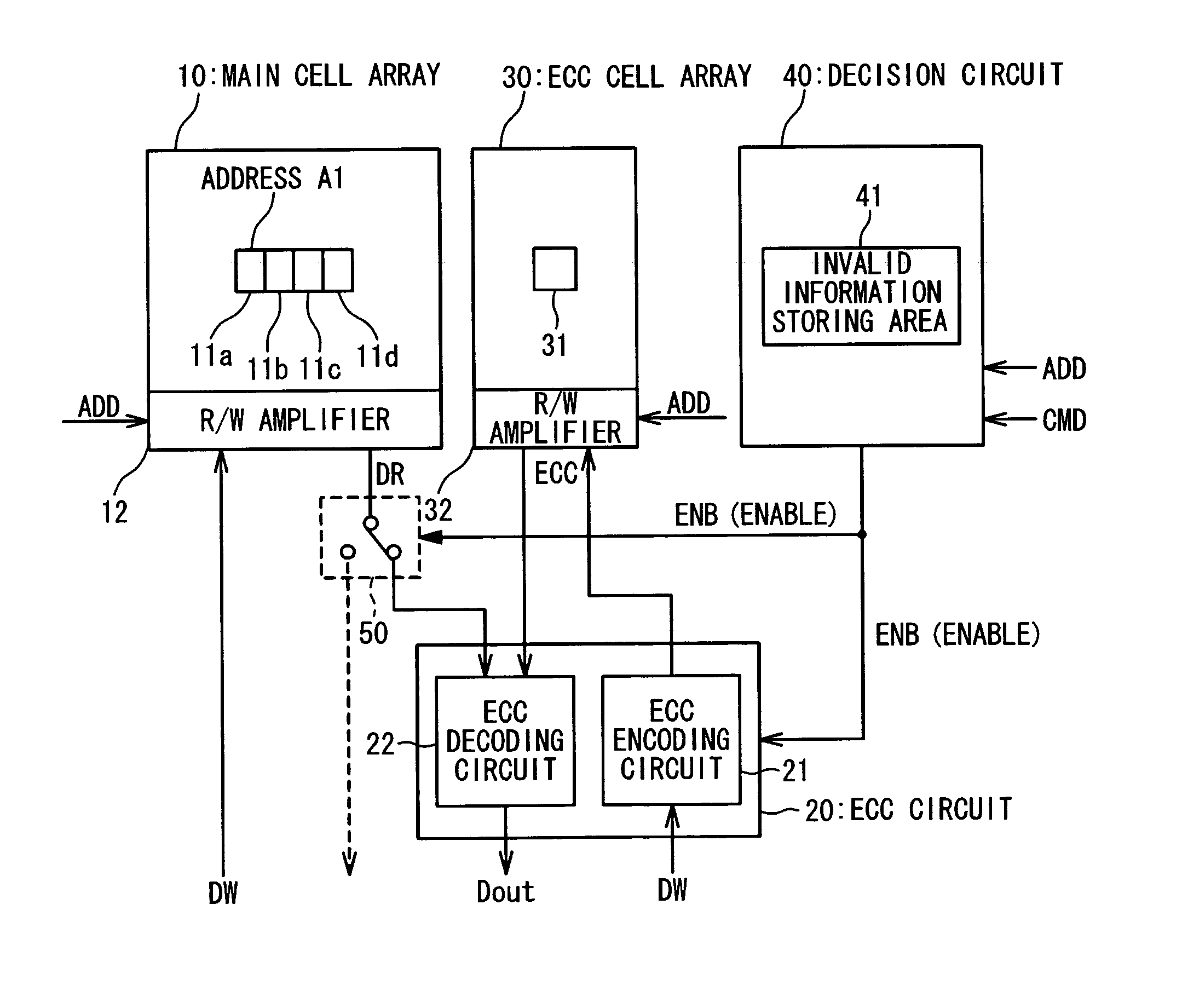
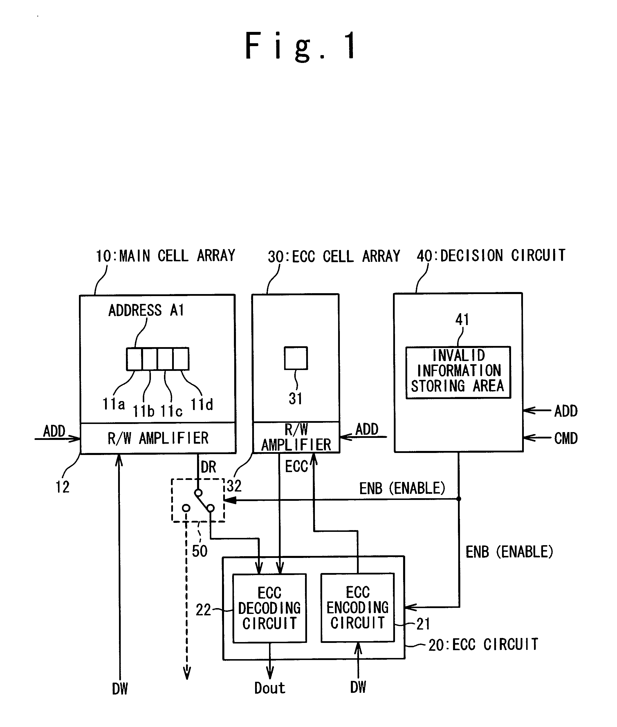
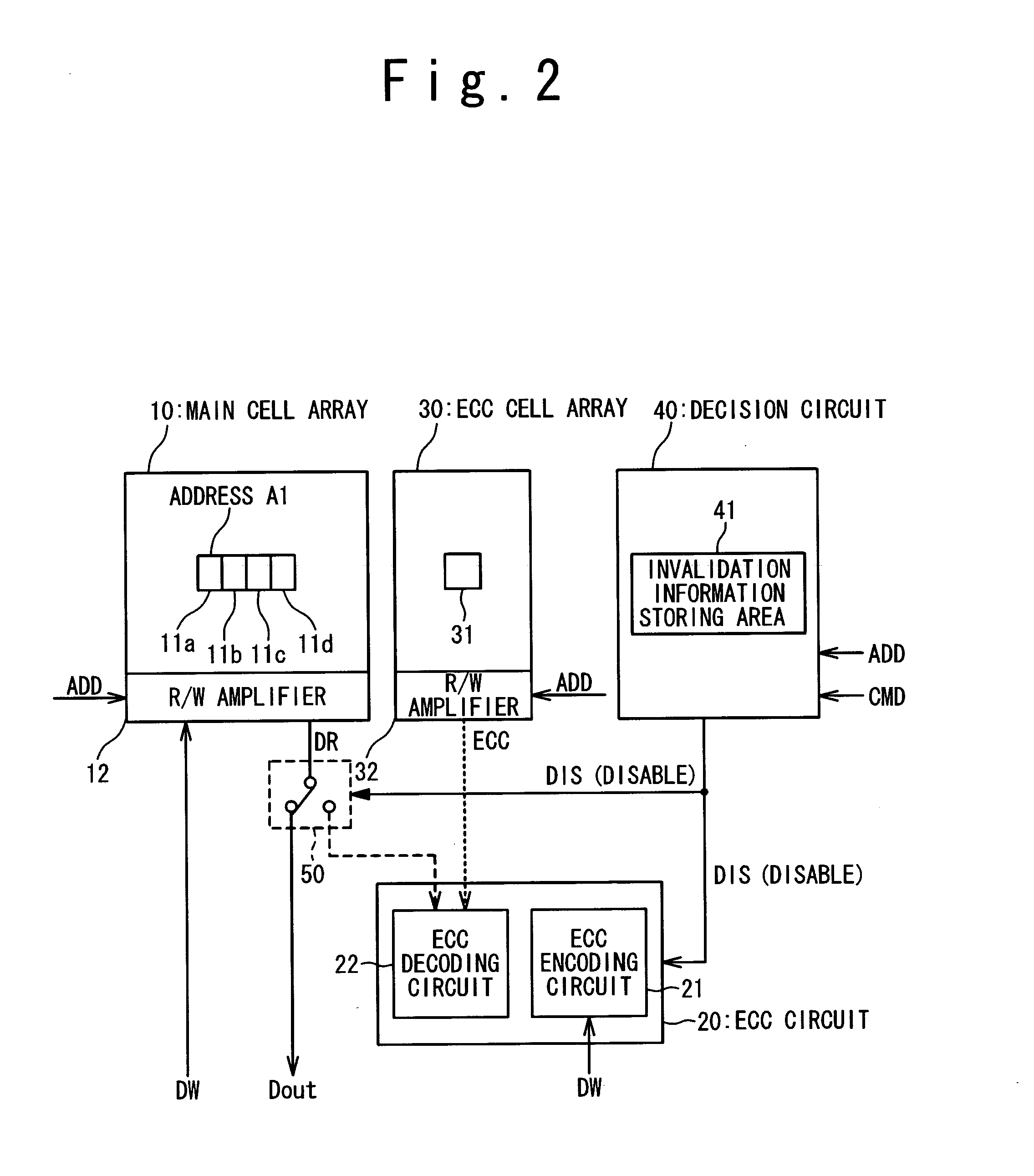
[0019] Embodiments of a semiconductor storage device according to the present invention will be described below with reference to the attached drawings. The semiconductor storage device according to the present invention is equipped with the ECC circuit.

1. Configuration and Functions

[0020] First, the configuration and the functions of the semiconductor storage device according to the embodiment of the present invention will be described referring to FIG. 1. In the following description, it is assumed that a data bus width is 32 bits.

[0021] A main cell array 10 is a storage area for storing data supplied from the outside of a memory, and has a plurality of m...


PUM


Abstract

A semiconductor memory device includes a memory cell array, an ECC (error correction code) circuit and a decision circuit. The ECC circuit calculates an error correction code for write data to be written in the memory cell array. The decision circuit invalidates the ECC circuit when a data width of the write data is less than a predetermined data width.

Description

BACKGROUND OF THE INVENTION [0001] 1. Field of the Invention [0002] The present invention relates to a semiconductor storage device. More particularly, the present invention relates to a semiconductor storage device equipped with an ECC function. [0003] 2. Description of the Related Art [0004] There is known an ECC (error correction code) circuit mounted on a semiconductor storage device such as a DRAM. The ECC circuit can not only detect a memory error merely but also specify a position (bit) of an error in data and correct it to a correct value. Specifically, the ECC circuit calculates information referred to as “error correction code (ECC)” to the data in writing the data. The calculated ECC is stored in a memory space. When the data is then read, the ECC circuit detects and corrects the error of the read data by referring to the ECC previously calculated. [0005] The data width of write data required for calculating the ECC is previously determined. For example, when a data bus w...

Claims


Application Information

Patent Timeline
Patent Type & Authority Applications(United States)
IPC IPC(8): G11C29/00
CPCG06F11/1052G11C7/1006G11C11/4076G11C11/4078G11C11/4087
Inventor TAKAHASHI, HIROYUKI
Owner RENESAS ELECTRONICS CORP
Why Eureka
Try Eureka