Memory devices including dielectric thin film and method of manufacturing the same

a technology of dielectric thin film and memory device, which is applied in the direction of semiconductor devices, capacitors, electrical devices, etc., can solve the problems of complex structure, high process temperature, and difficult to obtain high integration, and achieve high process temperature, simple manufacturing process, and high integration.

Active Publication Date: 2007-06-07
ELECTRONICS & TELECOMM RES INST
View PDF11 Cites 16 Cited by
  • Summary
  • Abstract
  • Description
  • Claims
  • Application Information

AI Technical Summary

Benefits of technology

[0010] The present invention is directed to a method of a manufacturing memory device, capable of manufacturing a non-volatile memory device using a simple manufacturing process. The present invention is also directed to a memory device, which can be highly integrated by a simple manufacturing process.

Problems solved by technology

However, since flash memory devices have a structure in which charge is accumulated on a floating gate in the presence of a strong electric field, the device structure becomes relatively complicated and difficult to densely integrate.
Consequently, thick interconnections are required, which again makes it difficult to obtain high integration.
However, materials such as Mn oxide layers disclosed in the cited documents (e.g., PrCaMnO, LaCaMnO, LaCaPbMnO, or the like) require a high process temperature and have complicated structures.
Consequently, manufactured strictures may easily deviate from what is necessary for the memory device to function properly.
Accordingly, such devices are difficult to manufacture.

Method used


Image

  • Memory devices including dielectric thin film and method of manufacturing the same
  • Memory devices including dielectric thin film and method of manufacturing the same
  • Memory devices including dielectric thin film and method of manufacturing the same

Examples


Embodiment Construction

[0024] Hereinafter, memory devices according to exemplary embodiments of the present invention will be described in detail with reference to accompanying drawings.

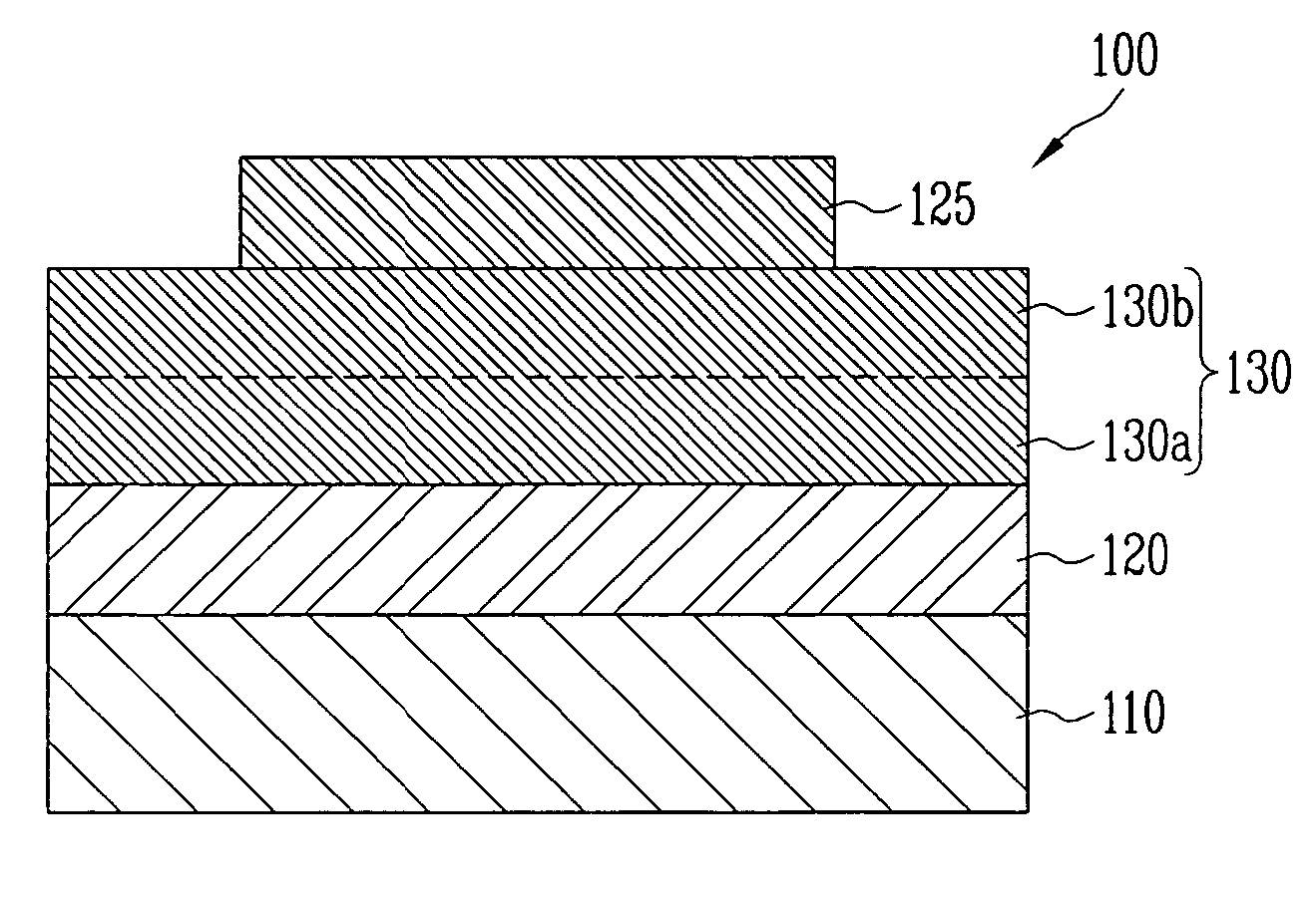
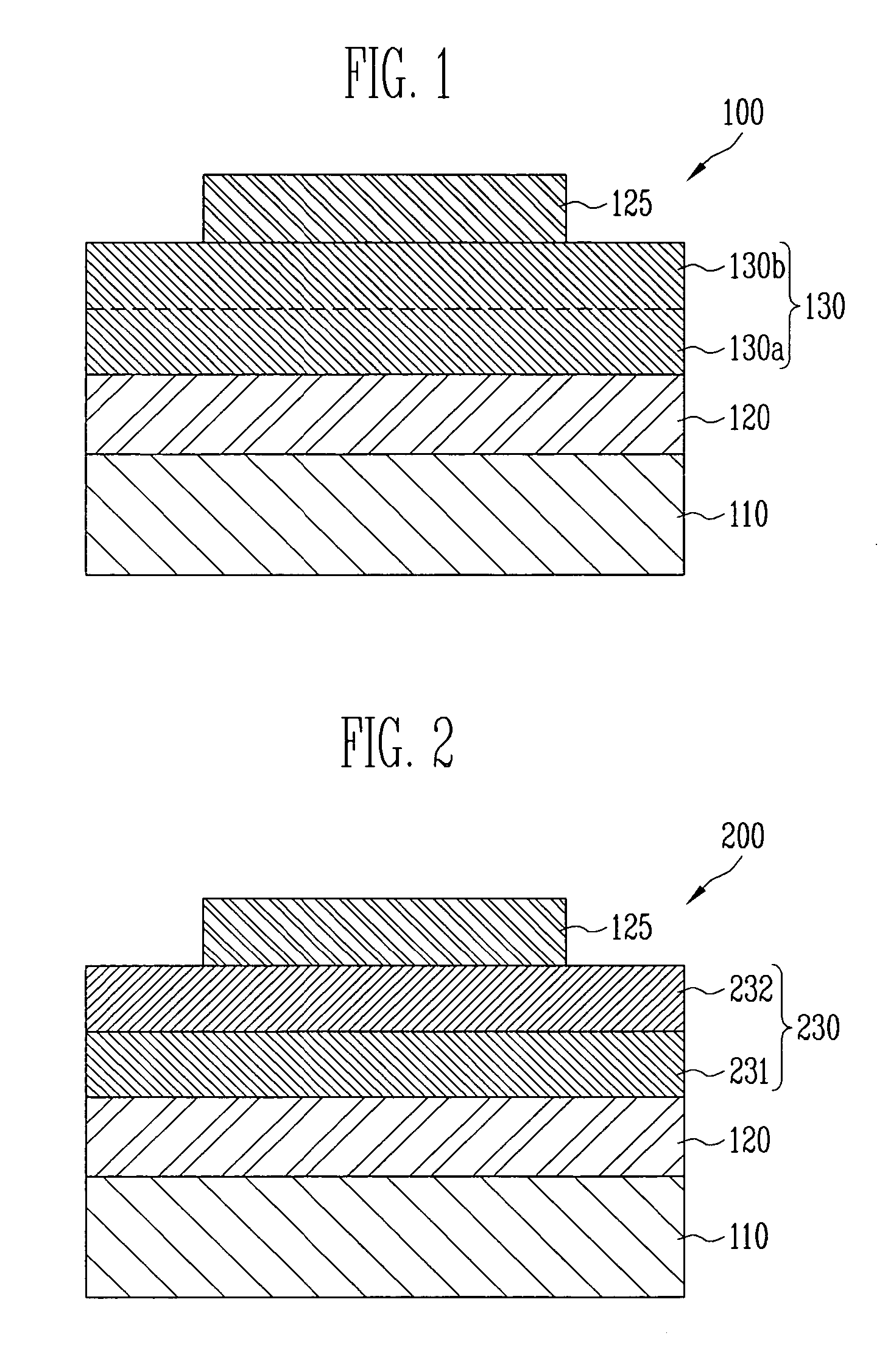
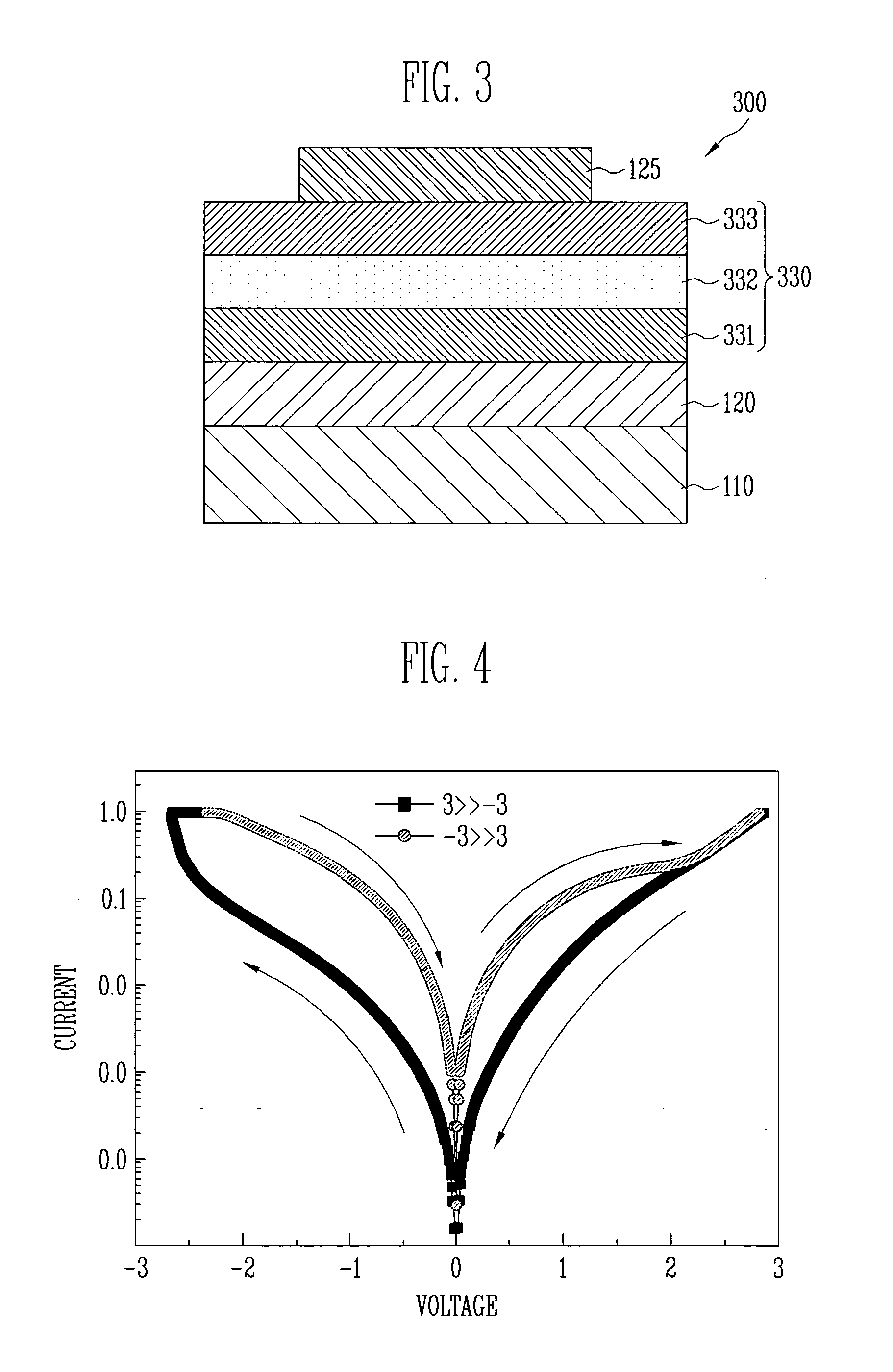
[0025]FIG. 1 is a schematic side cross-sectional view of a memory device having a dielectric thin film in accordance with an embodiment of the present invention. Referring to FIG. 1, the memory device 100 according to an embodiment of the present invention includes a substrate 110, a bottom electrode 120 disposed on the substrate 110, a dielectric thin film 130 disposed on the bottom electrode 120, and an top electrode 125 disposed thereon. The dielectric thin film 130 shown in FIG. 1 includes a lower dielectric layer 130a and an upper dielectric layer 130b.

[0026] The dielectric thin film 130 having a plurality of dielectric layers 130a and 130b using the same dielectric is shown in FIG. 1. As shown in FIG. 1, when the same dielectric is used, the dielectric layers having different trap charge densities can be formed by ...


PUM

PropertyMeasurementUnit
thicknessaaaaaaaaaa
dielectric constantaaaaaaaaaa

Abstract

A memory device including a dielectric thin film having a plurality of dielectric layers and a method of manufacturing the same are provided. The memory device includes: a bottom electrode; at least one dielectric thin film disposed on the bottom electrode and having a plurality of dielectric layers with different charge trap densities from each other; and an top electrode disposed on the dielectric thin film. Therefore, a memory device, which can be readily manufactured by a simple process and can be highly integrated using its simple structure, can be provided.

Description

CROSS-REFERENCE TO RELATED APPLICATION [0001] This application claims priority to and the benefit of Korean Patent Application Nos. 2005-117717, filed Dec. 5, 2005, and 2006-44063, filed May 17, 2006, the disclosures of which are incorporated herein by reference in their entirety. BACKGROUND [0002] 1. Field of the Invention [0003] The present invention relates to a memory device and a method of manufacturing the same, and more particularly, to a memory device including a dielectric thin film having a plurality of dielectric layers and a method of manufacturing the same. [0004] 2. Discussion of Related Art [0005] Non-volatile memory devices are information storage devices typically employed in cellular phones, digital cameras, MP3 players, and the like. The use of non-volatile memory devices in these and various other devices is extremely widespread, and demand for mass storage of data is recently increasing. In addition, non-volatile memory devices are commonly used in mobile device...

Claims


Application Information

Patent Timeline
Patent Type & Authority Applications(United States)
IPC IPC(8): H01L29/94
CPCH01G7/06H01L21/28282H01L21/28291H01L21/31637H01L21/31641H01L21/31645H01L21/31691H01L28/56H01L29/40117H01L29/40111H01L21/02197H01L21/022H01L21/02175
Inventor CHOI, SUNG-YOOLRYU, MIN KIKIM, ANSOONAH, CHIL SEONGYU, HAN YOUNG
Owner ELECTRONICS & TELECOMM RES INST
Why Eureka
Try Eureka