Organic el display

a technology of electroluminescent and organic el, applied in the direction of discharge tube luminescnet screen, discharge tube/lamp details, organic semiconductor devices, etc., can solve the problems of significant reduction in the lifetime of the organic el element, increase in power consumption, etc., and achieve the effect of improving the outcoupling efficiency of the organic el display

Inactive Publication Date: 2007-06-07
TOSHIBA MATSUSHITA DISPLAY TECH
View PDF5 Cites 15 Cited by
  • Summary
  • Abstract
  • Description
  • Claims
  • Application Information

AI Technical Summary

Benefits of technology

[0009] An object of the present invention is to improve an outcoupling efficiency of an organic EL display.

Problems solved by technology

However, if the current density is increased, power consumption increases and the lifetime of the organic EL element is significantly reduced.

Method used


Image

  • Organic el display
  • Organic el display
  • Organic el display

Examples


first embodiment

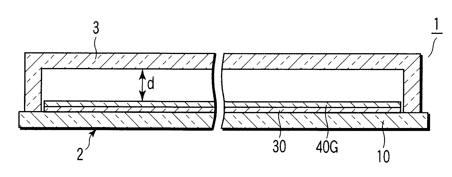
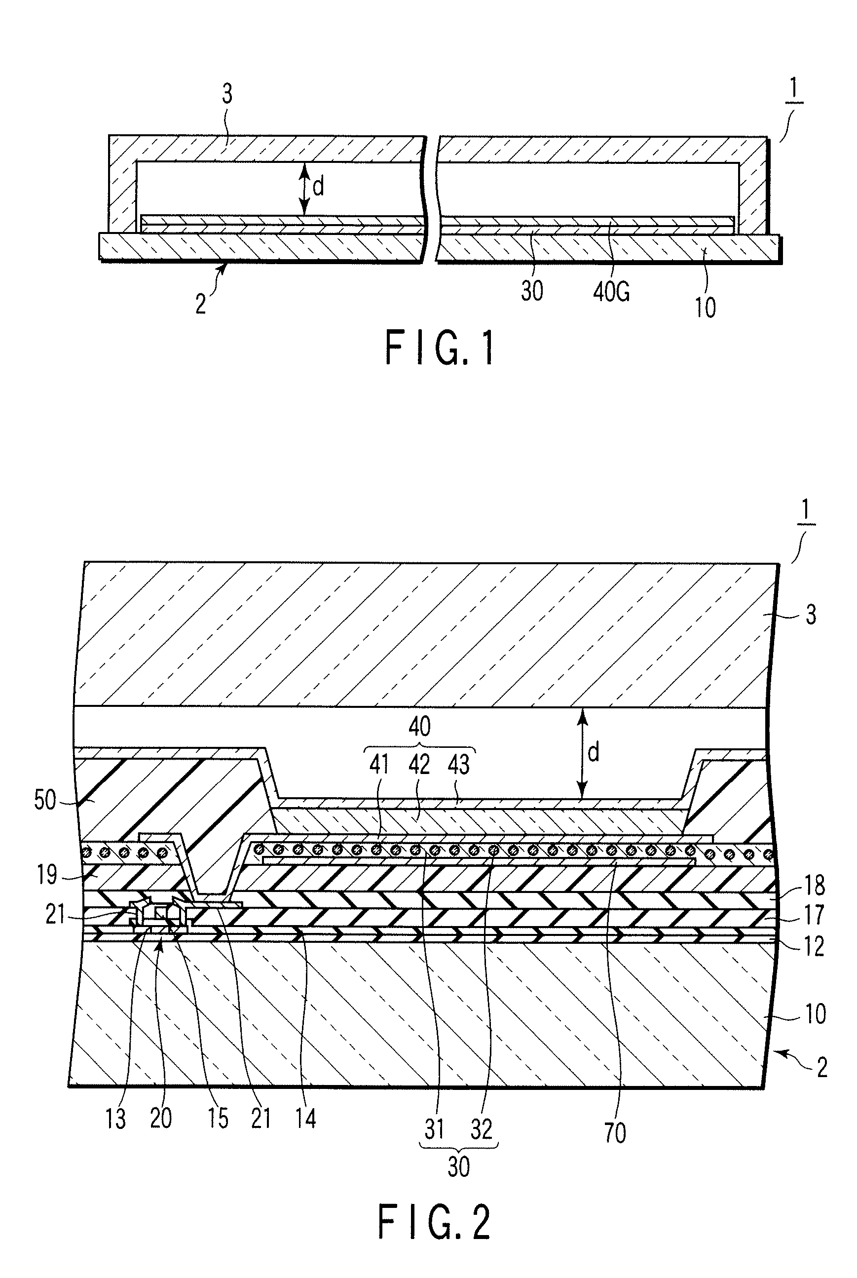
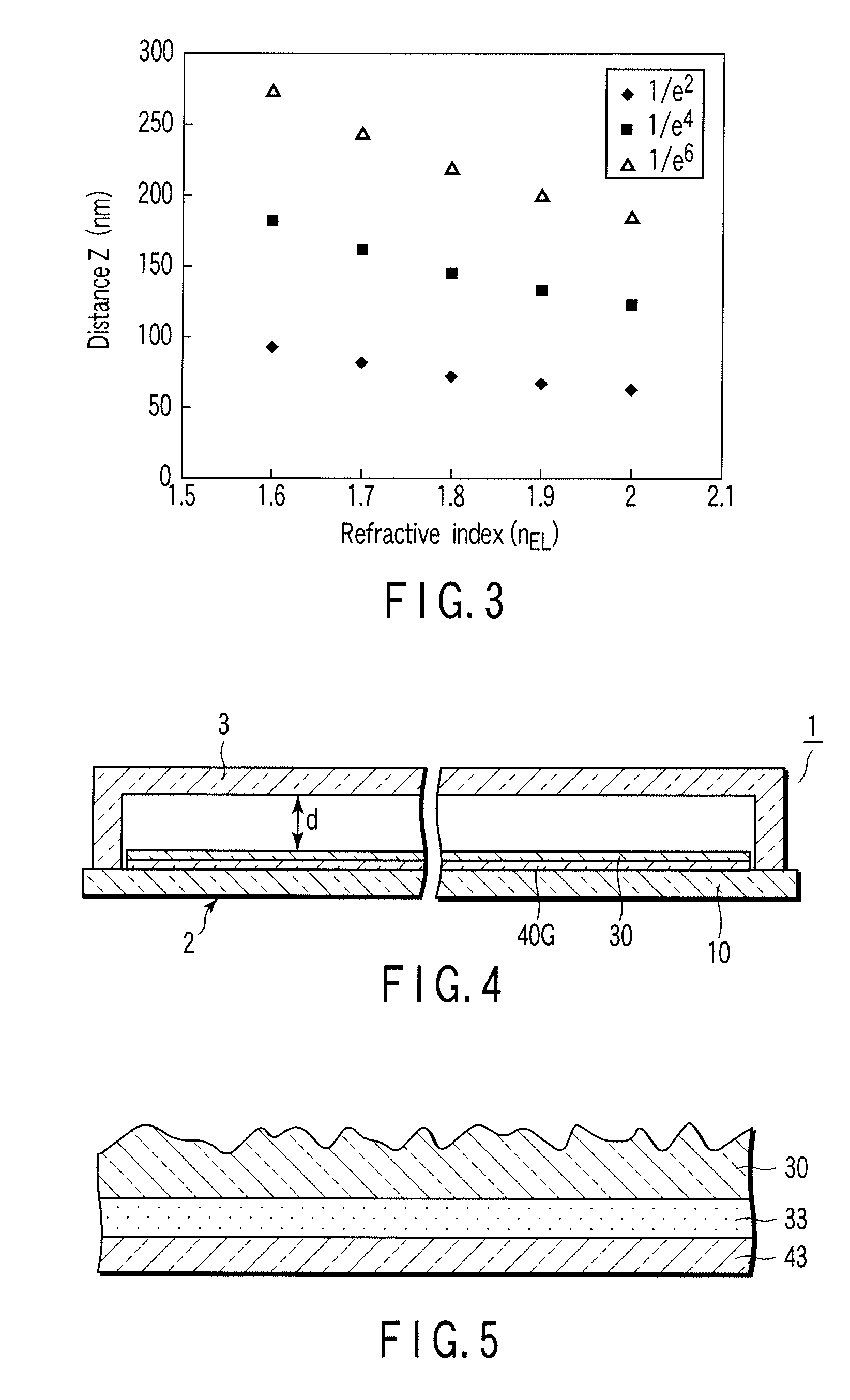
[0021]FIG. 1 is a cross sectional view schematically showing an organic EL display according to the present invention. FIG. 2 is a partial cross section showing an enlarged view of the organic EL display shown in FIG. 1. In FIGS. 1 and 2, the organic EL display 1 is illustrated such that its display surface, that is, the front surface, faces upwardly and the back surface faces downwardly.

[0022] The organic EL display 1 is a top emission organic EL display which employs an active matrix drive method. The organic EL display 1 includes an array substrate 2 and a sealing substrate 3.

[0023] For example, a surface of the sealing substrate 3 on the side of the array substrate 2 has a recessed shape. The array substrate 2 and the sealing substrate are joined together at peripheries thereof by means of, for example, adhesive or frit seal so as to form an enclosed space therebetween. The enclosed space is airtight and may be filled with an inert gas such as nitrogen gas or be evacuated.

[002...

second embodiment

[0053] the present invention will be described here.

[0054]FIG. 4 is a partial cross section schematically showing an organic EL display according to the second embodiment of the present invention. In FIG. 4, the organic EL display 1 is illustrated such that its display surface, that is, the front surface, faces upwardly and the back surface faces downwardly.

[0055] The organic EL display 1 has a structure similar to the organic EL display 1 shown in FIGS. 1 and 2 except that the outcoupling layer 30 is placed on a layer 40G which the organic EL elements 40 form. In a case where such a structure is employed, effects similar to those described in the first embodiment can be attained by setting the distance d from each element portion to the sealing substrate 3 in the same manner as described above.

[0056] In addition, the structure in which the outcoupling layer 30 is placed above the organic EL elements 40 makes it possible to eliminate the steps such as flattening and patterning the...


PUM


Abstract

A top emission organic EL display includes an array substrate including an insulating substrate, organic EL elements which are arranged on a main surface of the insulating substrate, and an outcoupling layer which extracts light components propagating in in-plane direction while causing multiple-beam interference from the organic EL element to make the light components travel in front of the organic EL element, and a sealing substrate facing and spaced apart from the organic EL elements. The display forms an enclosed space filled with an inert gas or evacuated between the sealing substrate and an element portion of the array substrate corresponding to the organic EL element. A distance between the element portion and the sealing substrate is 100 nm or longer.

Description

CROSS-REFERENCE TO RELATED APPLICATIONS [0001] This is a Continuation Application of PCT Application No. PCT / JP2005 / 017229, filed Sep. 13, 2005, which was published under PCT Article 21(2) in Japanese. [0002] This application is based upon and claims the benefit of priority from prior Japanese Patent Application No. 2004-279872, filed Sep. 27, 2004, the entire contents of which are incorporated herein by reference.BACKGROUND OF THE INVENTION [0003] 1. Field of the Invention [0004] The present invention relates to an organic electroluminescent (EL) display. [0005] 2. Description of the Related Art [0006] Since organic EL displays are of self-emission type, they have a wide viewing angle and a high repose speed. In addition, they do not require a backlight, and therefore, low-profile and lightweight are possible. For these reasons, the organic EL displays are attracting attention as a display which substitutes the liquid crystal display. [0007] An organic EL element, which is the main...

Claims


Application Information

Patent Timeline
Patent Type & Authority Applications(United States)
IPC IPC(8): H05B33/04H01J1/62
CPCB82Y20/00B82Y30/00H01L27/3244H01L51/5237H01L51/5268H01L2251/5315H01L2251/5369H10K59/12H10K50/8428H10K50/854H10K2102/3026H10K2102/331H01L21/67126H10K50/841H10K50/84H10K50/11
Inventor OKUTANI, SATOSHISANO, HIROSHISUNOHARA, KAZUYUKI
Owner TOSHIBA MATSUSHITA DISPLAY TECH
Why Eureka
Try Eureka