

Charge pump having shunt diode for improved operating efficiency
a technology of shunt diodes and discharge pumps, applied in the field of electric circuits, can solve the problems that the available semiconductor chip wafer surface might not allow shunt diodes to all nodes, and achieve the effect of reducing the impedance of the discharge pump and reducing the output charge ramp up tim
- Summary
- Abstract
- Description
- Claims
- Application Information
AI Technical Summary
Benefits of technology
Problems solved by technology
Method used
Image

Examples
Embodiment Construction
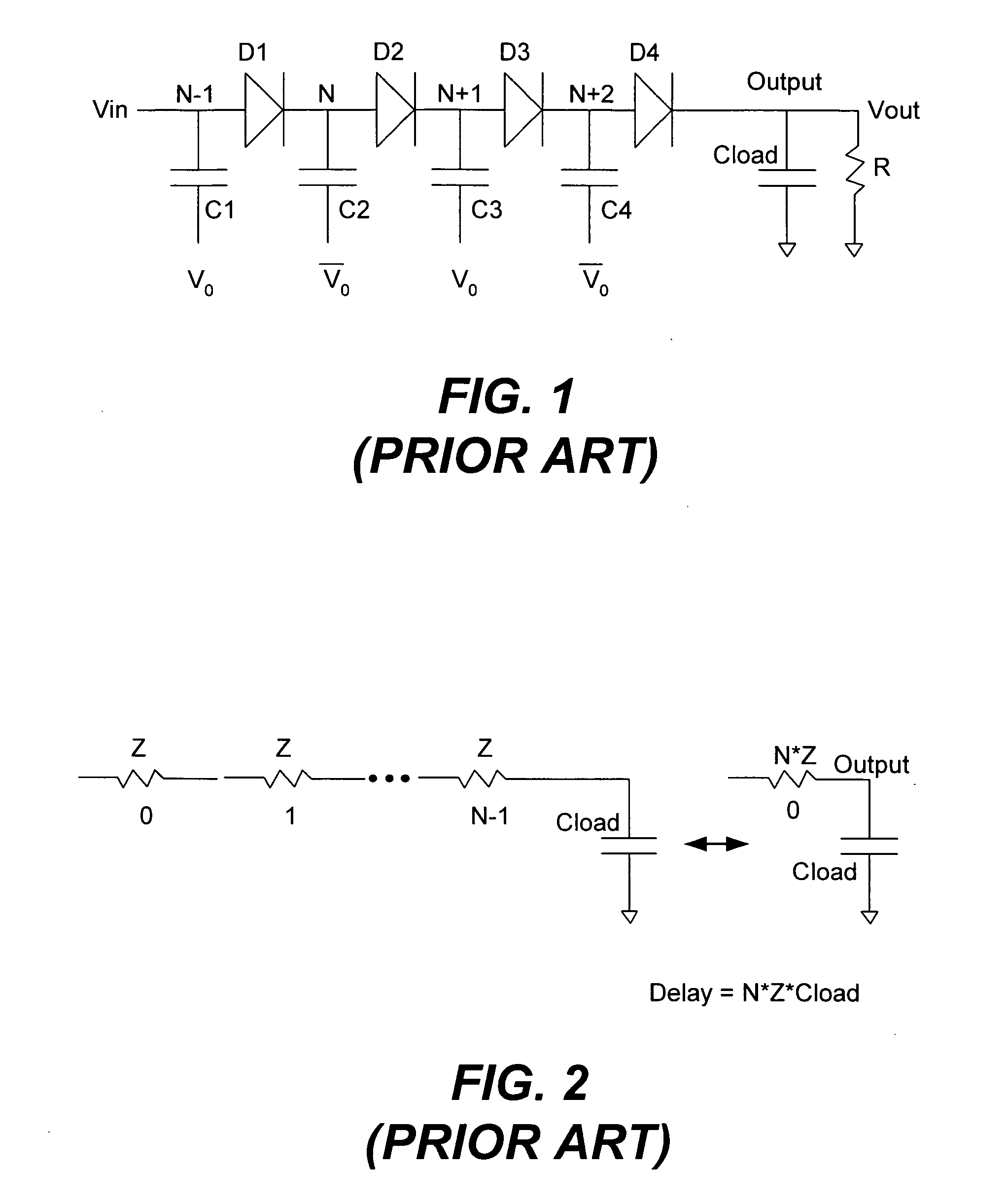
[0013] As noted above, the impedance of a charge pump is proportional to the number of stages in the charge pump chain. FIG. 2 is an equivalent electrical circuit of the conventional charge pump shown schematically in FIG. 1, where the impedance of each stage is given as Z. The impedance of an N stage charge pump will be approximately N·Z, as illustrated in FIG. 2.
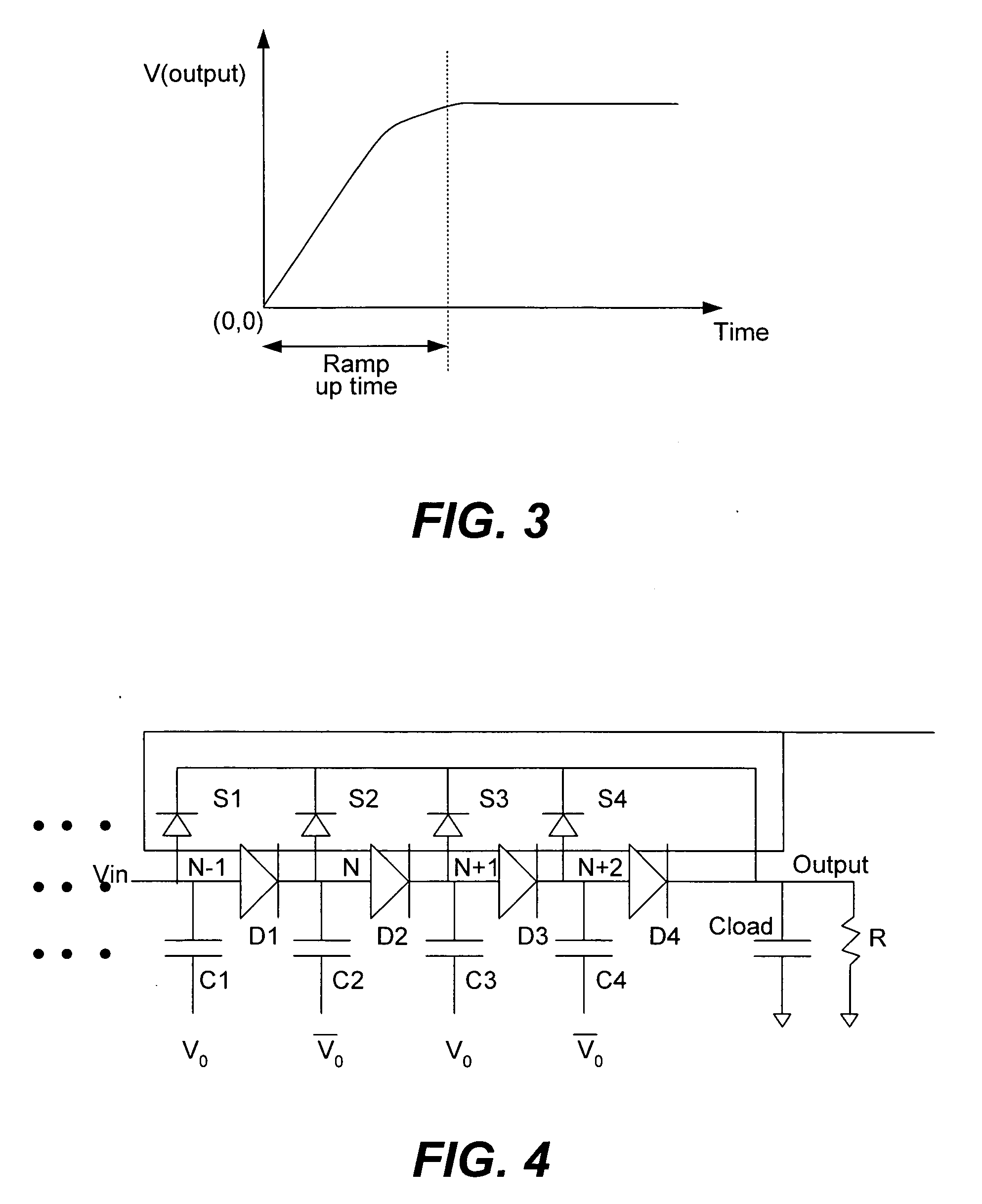
[0014] The output voltage ramp up time is proportional to the impedance of the charge pump. If the loading capacitance at the output terminal is Cload, the time constant is N Z Cload. The pump ramp up time is dependant on the initial voltage condition of the output terminal and the time constant N·Z·Cload, as illustrated in the plot of output voltage versus time in FIG. 3.
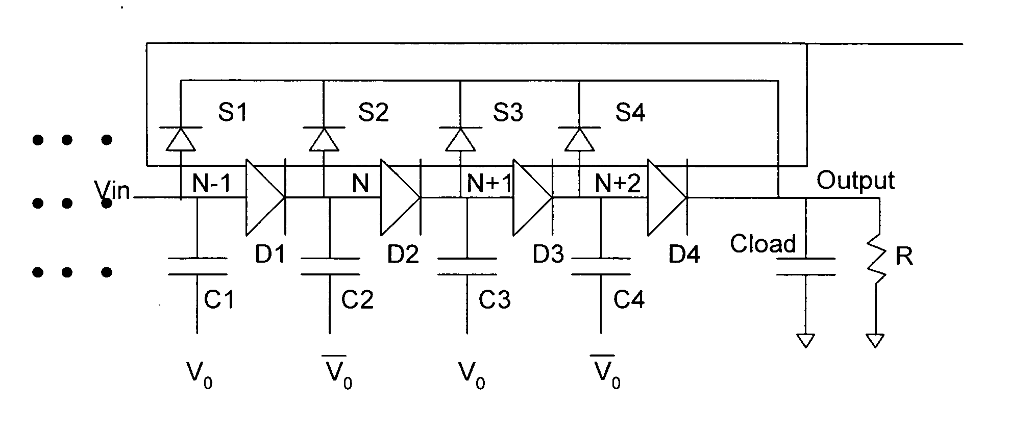
[0015] In accordance with the invention, one or more shunt diodes are connected between one or more nodes in the charge pump to the output terminal, as illustrated in FIG. 4. Here, the conventional charge pump illustrated in FIG. 1 is attended by adding...
PUM
 Abstract
Description
Claims
Application Information