Selective stress relaxation of contact etch stop layer through layout design

a technology of layout design and stress relaxation, applied in the direction of transistors, electric devices, solid-state devices, etc., can solve the problems of immense difficulties in conventional transistor scaling, and achieve the effect of reducing repetition

Inactive Publication Date: 2007-06-14
CHARTERED SEMICONDUCTOR MANUFACTURING
View PDF7 Cites 50 Cited by
  • Summary
  • Abstract
  • Description
  • Claims
  • Application Information

AI Technical Summary

Benefits of technology

[0033] The above and below advantages and features are of representative embodiments only, and are not exhaustive and/or exclusive. They are presented only to assist in understanding the invention. It should be understood that they are not representative of all the inventions defined by the claims, to be considered limitations on the invention as defined by the claims, or limitations on equivalents to the claims. For instance, some of these advantages may be mutually contradictory, in that they cannot be simultaneously present in a single embodiment. Similarly, some advanta...

Problems solved by technology

Conventional transistor scal...

Method used


Image

  • Selective stress relaxation of contact etch stop layer through layout design
  • Selective stress relaxation of contact etch stop layer through layout design
  • Selective stress relaxation of contact etch stop layer through layout design

Examples


first embodiment

mpressive (ESL) Stress Layer—

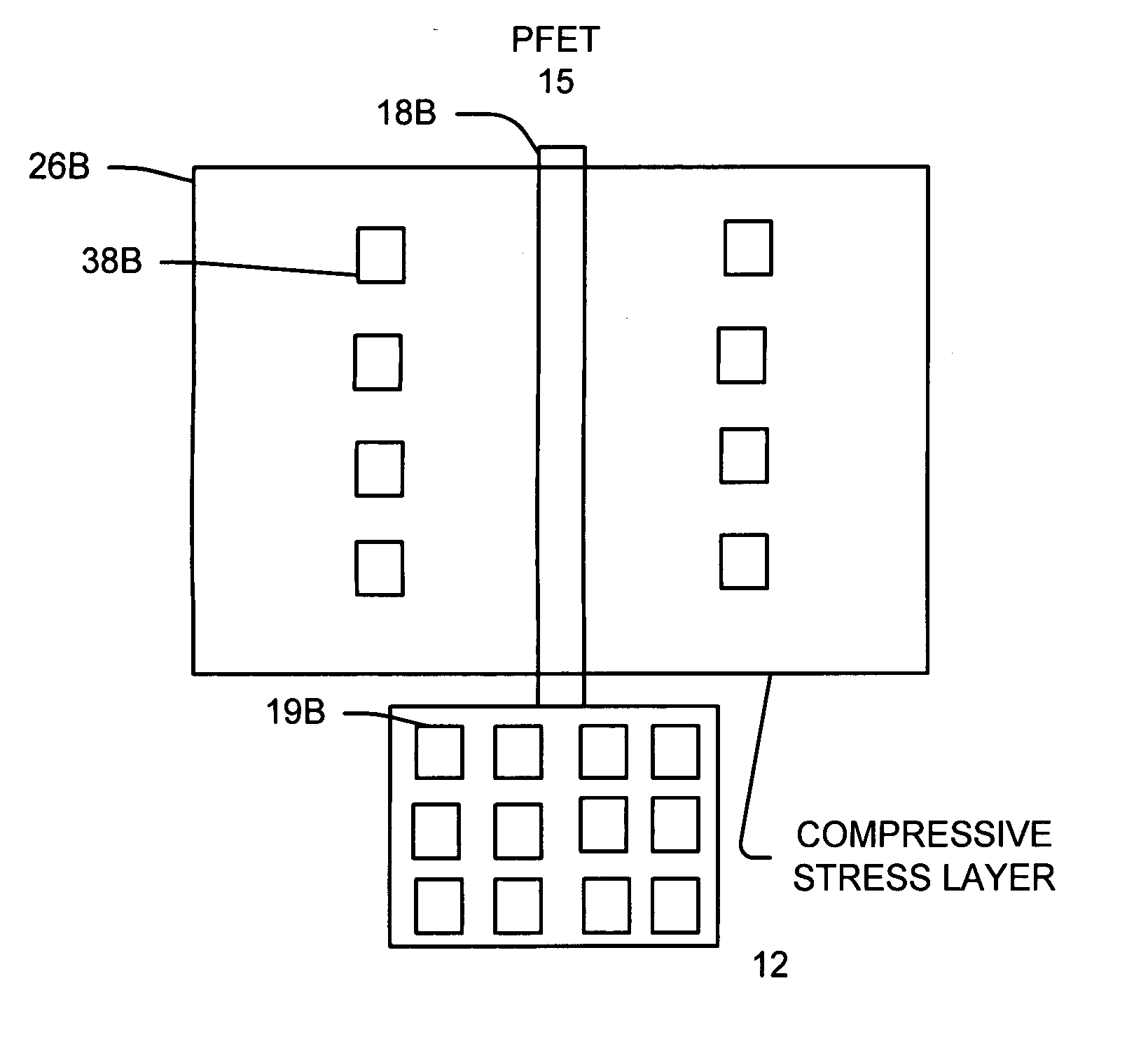
[0095]FIGS. 3A and 3B shows another example embodiment where the stress layer 30 is a compressive stress layer that induces a compressive stress on the channel regions.

[0096] The method and structure to form the MOS transistors and other devices is the same as described above. In this embodiment, the stress layer 30 has a compressive stress.

[0097] In an preferred option, the NMOS contact area is larger than the PMOS contact area so the compressive stress from the stress layer on the NMOS channel is less than the compressive stress on the PMOS channel.

[0098]FIG. 3B, shows an improvement of pFET using a highly compressive ESL coupled with a long contact via hole 38A (or closely packed multiple via) for the nFET the reduce the compressive stress on the NFET channel.

[0099] The transistor layout for nFET and pFET can be manipulated to relax the compressive stress of the ESL layer selectively on the nFET by using a long contact via to remove a large volume...

second example embodiment

and Compressive PMOS Stress Layer

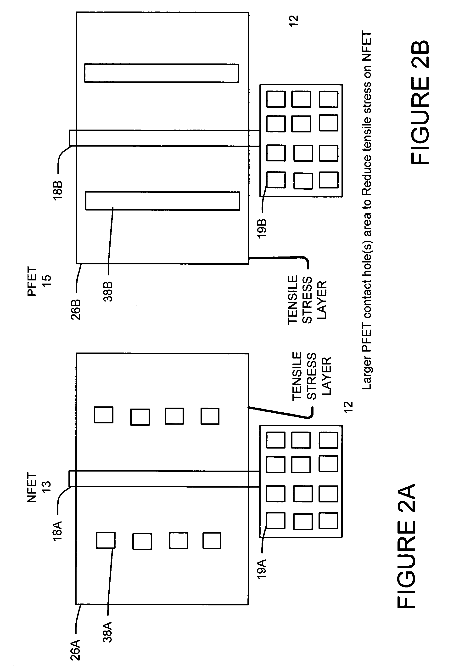
[0100] In a second example embodiment, the stress layer is comprised of a NMOS stress layer that is formed over the NMOS region and a PMOS stress layer formed over the PMOS region. The NMOS stress layer is a tensile stress layer that puts a tensile stress on the NMOS channel. The PMOS stress layer is a compressive stress layer that puts a compressive stress on said PMOS channel.

[0101] The stress layers and contact holes for the NMOS and PMOS are adapted and designed to obtain a predetermined stress for the NMOS and PMOS Tx.

[0102]FIGS. 4A and 4B show top down figures of the dual stress layers. FIG. 4A shows a PFET region 15 with a compressive stress layer over the PFET MOS and a NFET region 13 with a tensile stress layer over the NFET MOS TX. The contact holes are adapted to reduce or minimize the stress reducing effects of the contact hole on the stress layers.

[0103] For example, the stress layers and contact holes for the NMOS and PMOS are adapte...


PUM


Abstract

A structure and method of fabrication of a semiconductor device, where a stress layer is formed over a MOS transistor to put either tensile stress or compressive stress on the channel region. The parameters such as the location and area of the contact hole thru the stress layer are chosen to produce a desired amount of stress to improve device performance. In an example embodiment for a tensile stress layer, the PMOS S/D contact area is larger than the NMOS S/D contact area so the tensile stress on the PMOS channel is less than the tensile stress on the NMOS channel. In an example embodiment for a compressive stress layer, the NMOS contact area is larger than the PMOS contact area so that the compressive stress on the NMOS channel is less than the compressive stress on the PMOS channel.

Description

BACKGROUND OF INVENTION [0001] 1) Field of the Invention [0002] This invention relates generally to structures and methods for making semiconductor devices and more particularly to the structures and methods for semiconductor devices having stress layers. [0003] 2) Description of the Prior Art [0004] Conventional transistor scaling is facing immense difficulties. One way to enhance transistor performance is through the Improvements in performances of MOS transistors and CMOS have been made by shrinkage or scaling down,thereof, for example, shortening a channel length and a reduction in thickness of a gate insulating film. A reduction in thickness of the gate insulating film and a minimum size or dimension for process have become closer to the limitations. A further improvement in performance can not depend upon the limited shrinkage or scaling down of the device, but should depend upon any other measures than the shrinkage or scaling down of the device. [0005] One of the improvement...

Claims


Application Information

Patent Timeline
IPC IPC(8): H01L29/78H01L21/8238
CPCH01L21/76816H01L21/76829H01L21/823807H01L21/823814H01L21/823871H01L27/0207H01L29/665H01L29/6659H01L29/7843
Inventor TEO, LEE WEEQUEK, ELGINSOHN, DONG KYUN
Owner CHARTERED SEMICONDUCTOR MANUFACTURING
Why Eureka
Try Eureka