
Isolation method of defining active fins, method of fabricating semiconductor device using the same and semiconductor device fabricated thereby

Inactive Publication Date: 2007-06-14
SAMSUNG ELECTRONICS CO LTD
View PDF13 Cites 115 Cited by
  • Summary
  • Abstract
  • Description
  • Claims
  • Application Information

AI Technical Summary

Benefits of technology

[0038] In another aspect, the present invention is directed to a semiconductor device comprising: a plurality of active fins on a semiconductor substrate; a liner pattern surrounding lower sidewalls of the active fins; a gate dielectric layer surrounding higher sidewal

Problems solved by technology

In a planar-type transistor, however, increasing the width of the active region runs counter to recent trends toward higher device integration.
Thus, it is not only disadvantageous for downsizing a device, but also difficult to restrain the short channel effect.
This can cause degradation of current drivability of the Fin-FET devices.
As a result, the gate electrodes locally increase the electric potential in electrically unrelated active regions and thus can cause degradation of the electrical properties of the Fin-FET device.

Method used


Image

  • Isolation method of defining active fins, method of fabricating semiconductor device using the same and semiconductor device fabricated thereby
  • Isolation method of defining active fins, method of fabricating semiconductor device using the same and semiconductor device fabricated thereby
  • Isolation method of defining active fins, method of fabricating semiconductor device using the same and semiconductor device fabricated thereby

Examples


Embodiment Construction

[0050] The present invention will now be described more fully hereinafter with reference to the accompanying drawings, in which exemplary embodiments of the invention are shown. This invention may, however, be embodied in different forms and should not be construed as limited to the exemplary embodiments set forth herein. Rather, these exemplary embodiments are provided so that this disclosure will be thorough and complete, and will fully convey the scope of the invention to those skilled in the art. In the drawings, the thickness of layers and regions may be exaggerated for clarity, and like numbers refer to like elements throughout.

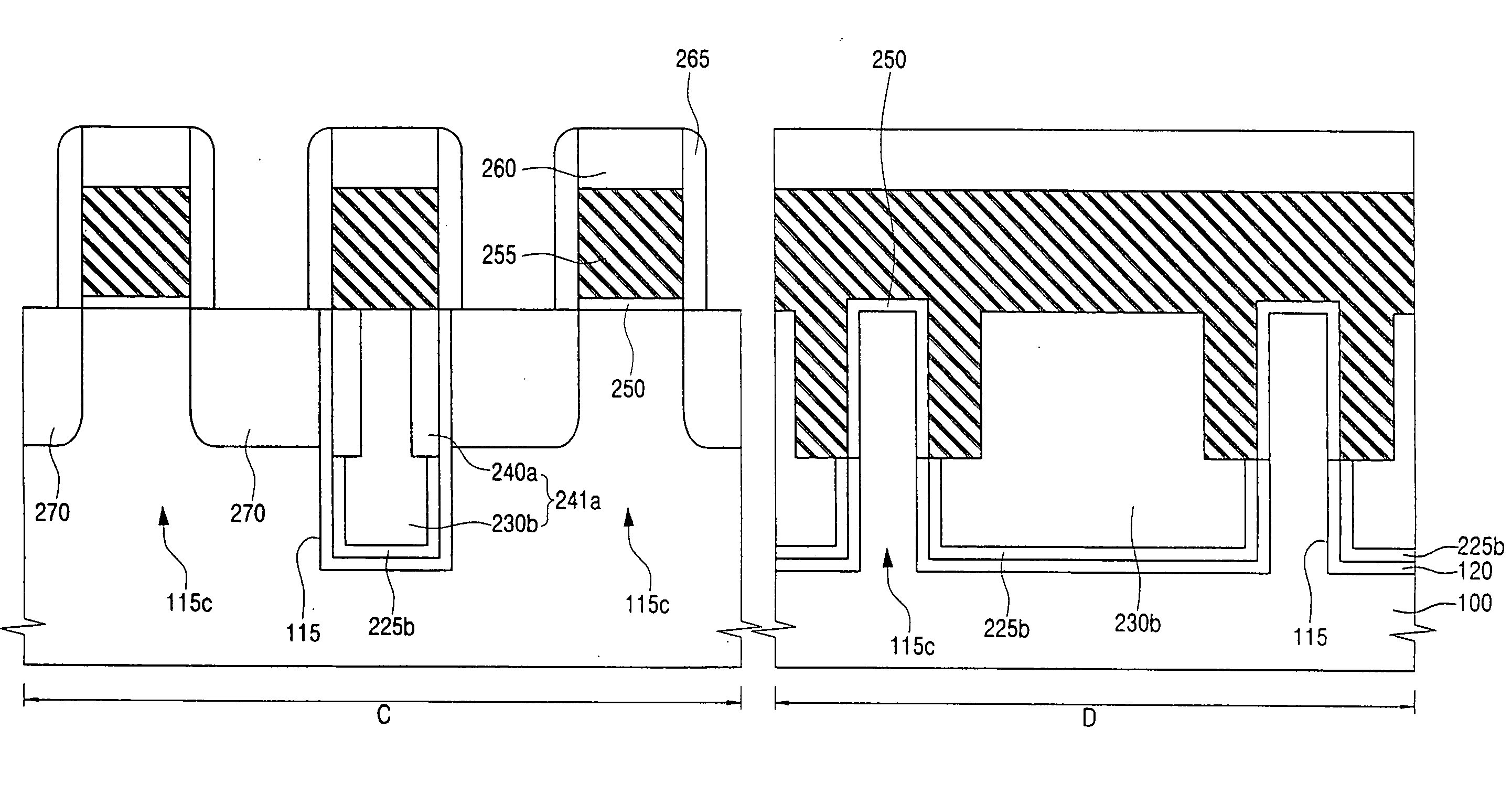
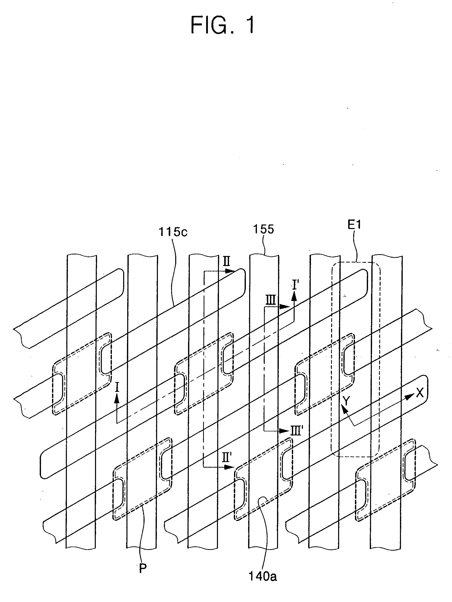
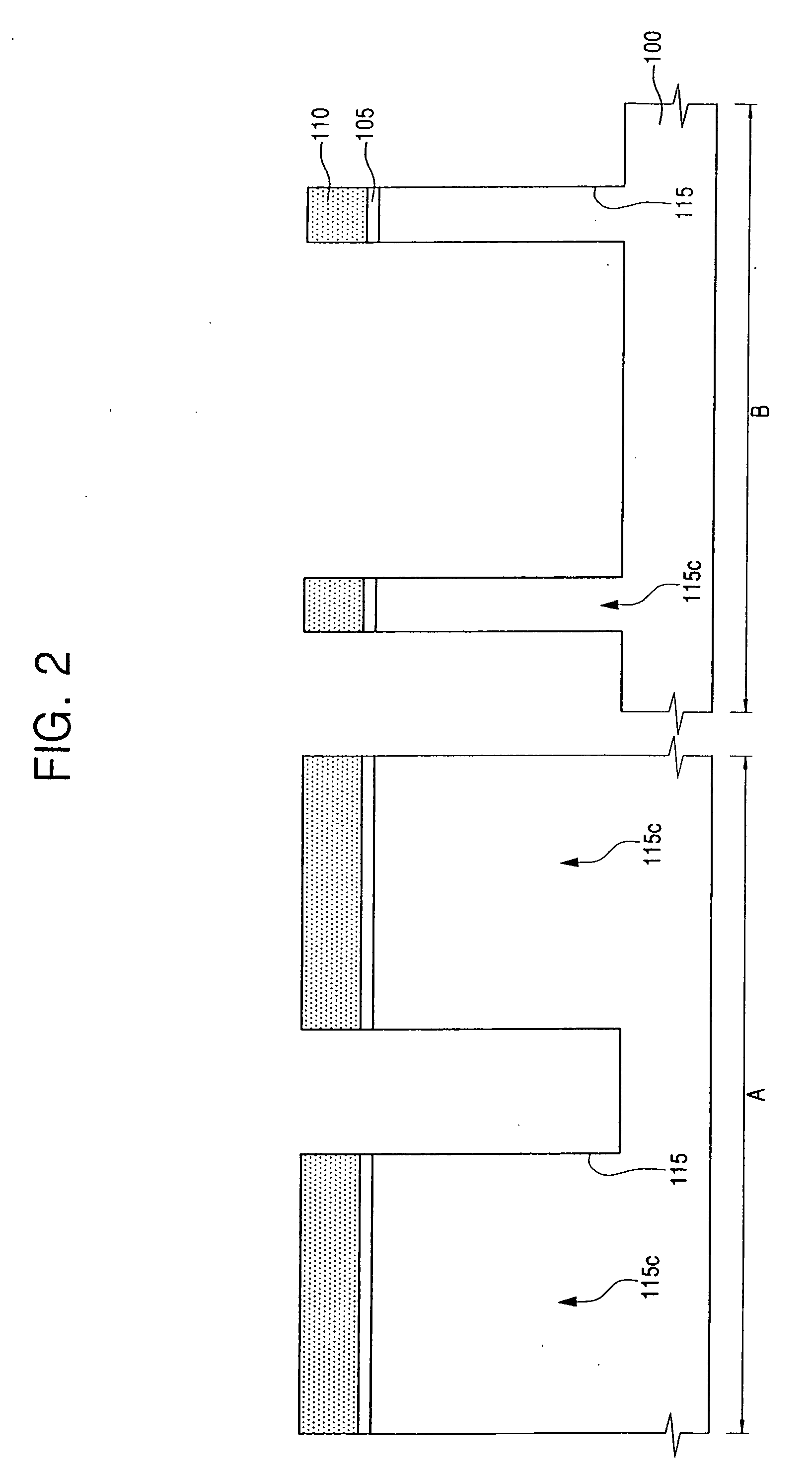
[0051]FIG. 1 is a plan view of a semiconductor device according to an exemplary embodiment of the invention, and FIGS. 2 through 9 are cross-sectional views illustrating a method of fabricating a semiconductor device according to an exemplary embodiment of the invention. In FIGS. 2 through 8, reference mark “A” denotes a cross-section taken along line ...


PUM


Abstract

An isolation method of defining active fins, a method of fabricating a semiconductor device using the same, and a semiconductor device fabricated thereby are provided. The method of fabricating a semiconductor device includes: preparing a semiconductor substrate; and forming a plurality of active fins having major and minor axes and two-dimensionally arrayed on the semiconductor substrate in directions of the major and minor axes. A liner pattern is formed on lower sidewalls of the active fins. An isolation layer is formed on the semiconductor substrate having the liner pattern, and the isolation layer exposes top surfaces of the active fins and a part of the active fins' sidewalls substantially parallel to the major axis. Parallel gate lines are formed to cover the top surfaces and the exposed sidewalls of the active fins, cross over the active fins, and run on the isolation layer.

Description

CROSS-REFERENCE TO RELATED APPLICATION [0001] This application claims priority to Korean Patent Application No. 10-2005-0123188, filed on Dec. 14, 2005, the contents of which are incorporated herein by reference in their entirety. BACKGROUND OF THE INVENTION [0002] 1. Field of the Invention [0003] The present invention relates to a semiconductor device, and more particularly, to an isolation method of defining active fins, a method of fabricating a semiconductor device using the same, and a semiconductor device fabricated thereby. [0004] 2. Description of the Related Art [0005] Semiconductor devices widely adopt a discrete device such as a field effect transistor as a switching device. In the transistor, an operating speed of the device is determined by an on-current generated in a channel between a source and a drain. Generally, a gate electrode and the source / drain are formed in a device formation region, i.e., an active region, of a semiconductor substrate in order to form a plan...

Claims


Application Information

Patent Timeline
IPC IPC(8): H01L21/76H01L29/00H01L21/4763
CPCH01L21/823437H01L21/823481H01L21/823821H01L29/66795H01L29/7851H01L21/76
Inventor KIM, KEUN-NAMLEE, CHULCHO, EUN-SUK
Owner SAMSUNG ELECTRONICS CO LTD
Learn More