System and method for message passing fabric in a modular processor architecture

a message and fabric technology, applied in the field of message based interconnection system and method, can solve the problems of not being able to be dynamically changed, not being well-suited for a semiconductor architecture, and not being able to adapt and dynamically optimize for a range of tasks

Inactive Publication Date: 2007-06-21
GATECHANGE TECH
View PDF4 Cites 31 Cited by
  • Summary
  • Abstract
  • Description
  • Claims
  • Application Information

AI Technical Summary

Benefits of technology

[0009] The present invention provides a programmable logic device, more specifically a programmable integrated circuit interconnect system and method. The present invention provides for a system and method of providing a message passing fabric in a modular processing system that comprises generally a plurality of processing elements, or VFBs, which are configured to access other available processing elements. The processing elements of the present invention communicate with a plurality of message ports, or busses, such that message ports on adjacent, which does not necessarily mean physically adjacent, processing elements define a message path between the processin

Problems solved by technology

The main problem with conventional integrated circuit interconnect structures is their inability to be adaptable to and dynamically optimized for a range of tasks.
Another problem with conventional integrated circuit interconnect structures is their inability to be dynamically changed to precisely meet the requirements of the current task or set of tasks at hand and then be modified should the task or tasks change.
While the programmable interconnect within FPGA-type devices can in theory be reconfigured, in practice this is rarely done because of the complexity of the tools required and the time lapse (“configuration latency”) associated with such changes.
Another problem with conventional integrated circuit interconnect structures is that they are not well-suited for a semiconductor architecture wherein the data paths are constantly changing.
Furthermore, conventional fixed and programmable routing structures do not allow an array of functions—either homogenous or heterogeneous—to be quickly and easily laid out in a de

Method used


Image

  • System and method for message passing fabric in a modular processor architecture
  • System and method for message passing fabric in a modular processor architecture
  • System and method for message passing fabric in a modular processor architecture

Examples


Embodiment Construction

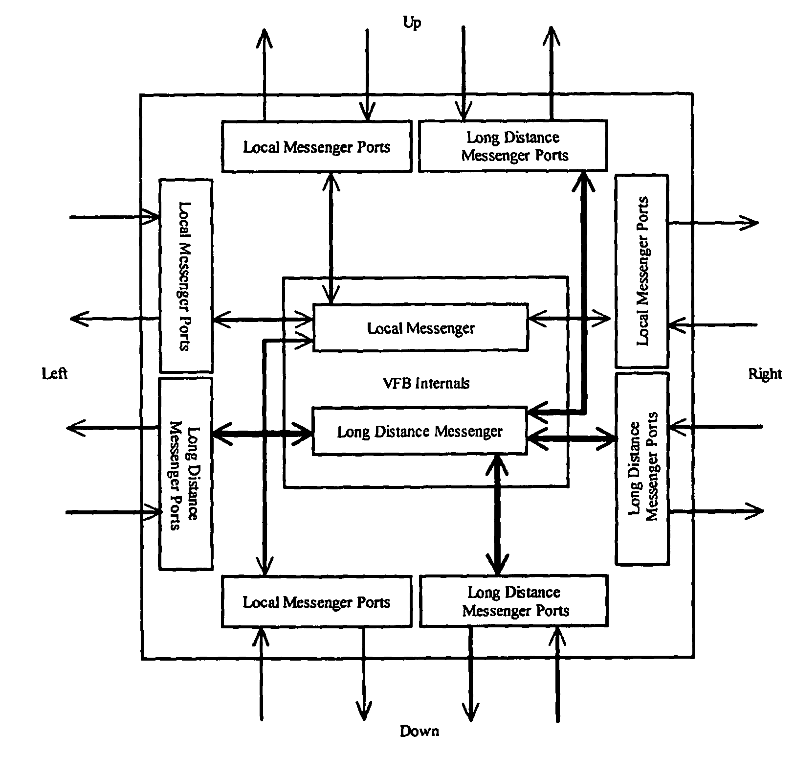
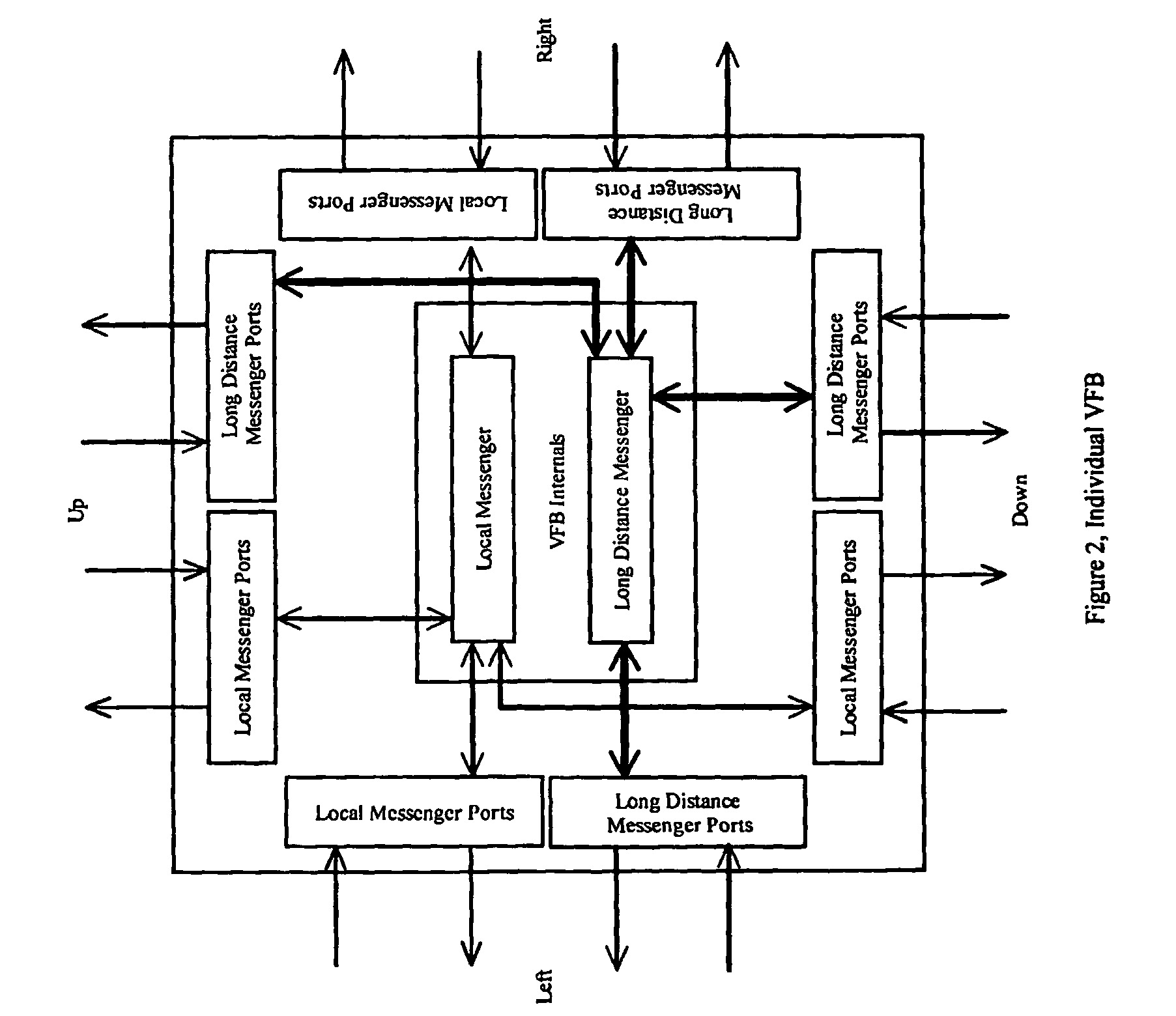
[0030] Throughout the figures provided, numbering is preserved such that a reference number appearing in more than one figure refers to the same object. Arrows within the figures refer to the primary direction of the flow of control and data and should not be construed as the sole direction of data flow.

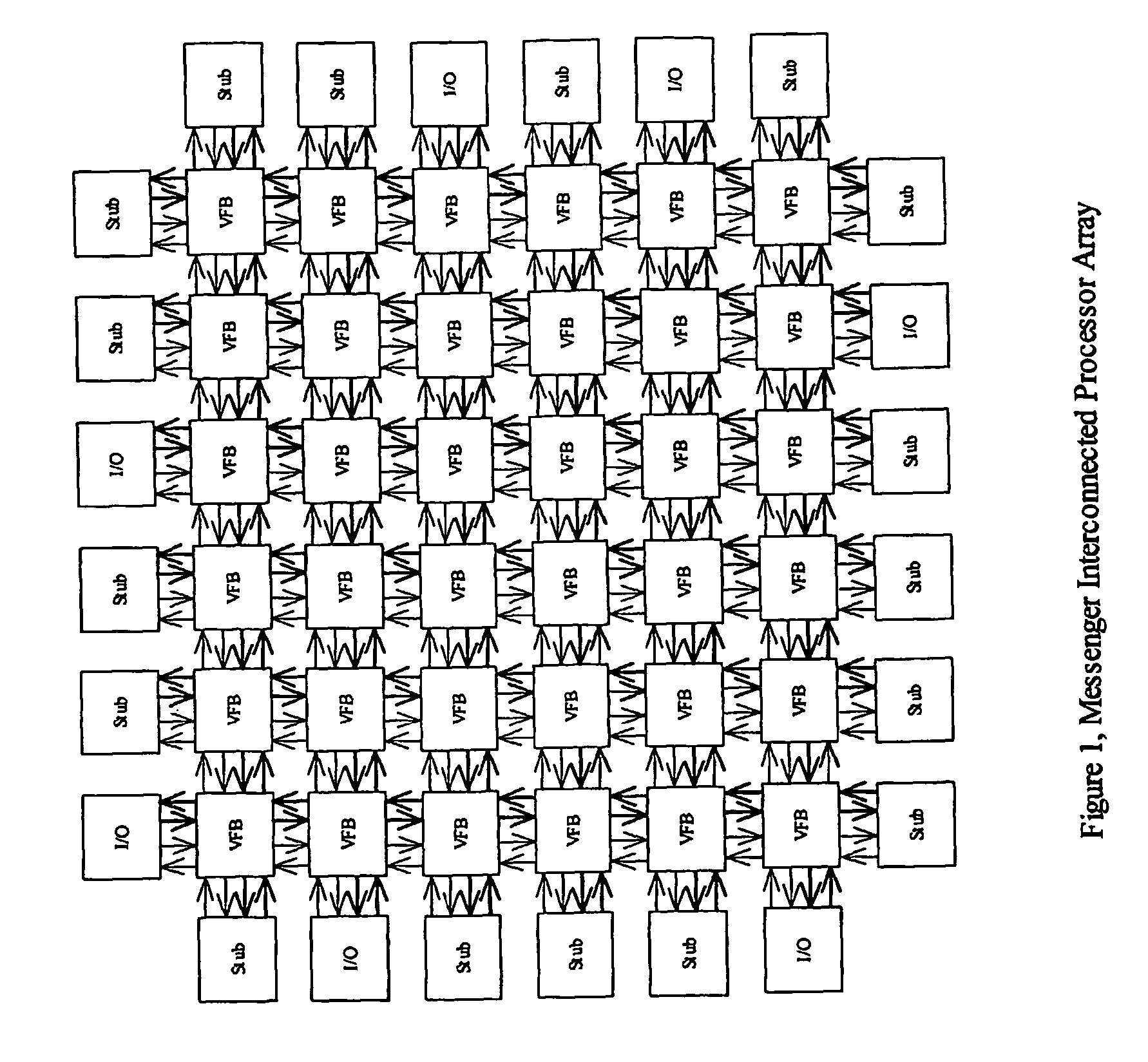
[0031] Referring now to the Figures, various preferred embodiments of the present invention are shown. Generally, as illustrated in FIG. 1, the modular processor architecture of the present invention comprises at least one processing element. More preferably the architecture comprises a plurality of processing and / or logic elements 101(also known as Virtual Function Blocks or VFBs, and hereinafter referred to as VFBs) configured to be interconnected according to a preferred message passing fabric system and method. In a plurality of preferred embodiments of the present invention, the processing and / or logic elements, VFBs (101) to be interconnected, are configured to interconnect wi...


PUM


Abstract

The invention provides a system and method of providing a message passing fabric in a modular processing system where a plurality of processing elements (VFBs), access other available processing elements to provide a message passing fabric where the fabric asynchronously establishes routes for synchronous messages from an origin processing element to a destination processing element to permit an operation to occur at the destination processing element in a flexible, efficient, self-routing and real-time dynamically optimized manner.

Description

CROSS REFERENCE TO RELATED APPLICATIONS [0001] This application claims benefit under 35 U.S.C. Section 119(e) from the following Provisional Applications, Provisional Application No. 60 / 519,129 filed Nov. 12, 2003 and Provisional Application No. 60 / 562,908 filed Apr. 16, 2004, of which the entire contents of both applications are herein incorporated by reference.BACKGROUND OF THE INVENTION [0002] The present invention relates generally to a system and method for message based interconnect in electrical or electronic devices. More specifically, the present invention relates to a system and method for a message passing fabric in a modular processor architecture where the architecture consists of a self-routing, message-based interconnect system for electrical and / or electronic devices. [0003] It can be appreciated that integrated circuits (chips or ICs) with various types of interconnect have been in use for years. Typical integrated circuit interconnections can be grouped into three ...

Claims


Application Information

Patent Timeline
IPC IPC(8): G06F15/00G06F9/44H04L
CPCG06F15/16H04L49/35H04L49/1507
Inventor HORTON, JAMES A.KLEIN JR., ROBERT C.GROSS, GEORGE F.FLEMMING, TERRYJENKINS JR., REYNOLDS E.
Owner GATECHANGE TECH
Why Eureka
Try Eureka