CMOS Image Sensor and Manufacturing Method Thereof

a technology of image sensor and manufacturing method, which is applied in the field of image sensor, can solve the problems of degrading image sensor characteristics and noise, and achieve the effects of enhancing photosensitivity, minimizing noise components, and improving condensing performan

Inactive Publication Date: 2007-06-28
DONGBU ELECTRONICS CO LTD
View PDF6 Cites 10 Cited by
  • Summary
  • Abstract
  • Description
  • Claims
  • Application Information

AI Technical Summary

Benefits of technology

[0020]An object of the present invention is to provide a CMOS image sensor capable of enhancing the photosensitivity by minimizing noise components.
[0021]A second object of the present invention is to provide a CMOS image sensor capable of improving a condensing performance.

Problems solved by technology

However, the CMOS image sensor according to the related art has the following problems.
The thickness of the second planarization layer can degrade the characteristics of the image sensor.
For example, noise can be caused by light being incident on unintended photodiodes.

Method used


Image

  • CMOS Image Sensor and Manufacturing Method Thereof
  • CMOS Image Sensor and Manufacturing Method Thereof
  • CMOS Image Sensor and Manufacturing Method Thereof

Examples


Embodiment Construction

[0032]Reference will now be made in detail to the preferred embodiments of the present invention, examples of which are illustrated in the accompanying drawings. Wherever possible, the same reference numbers will be used throughout the drawings to refer to the same or like parts.

[0033]Hereinafter, a CMOS image sensor and a method for manufacturing the same according to an embodiment of present invention will be described with reference to the accompanying drawings.

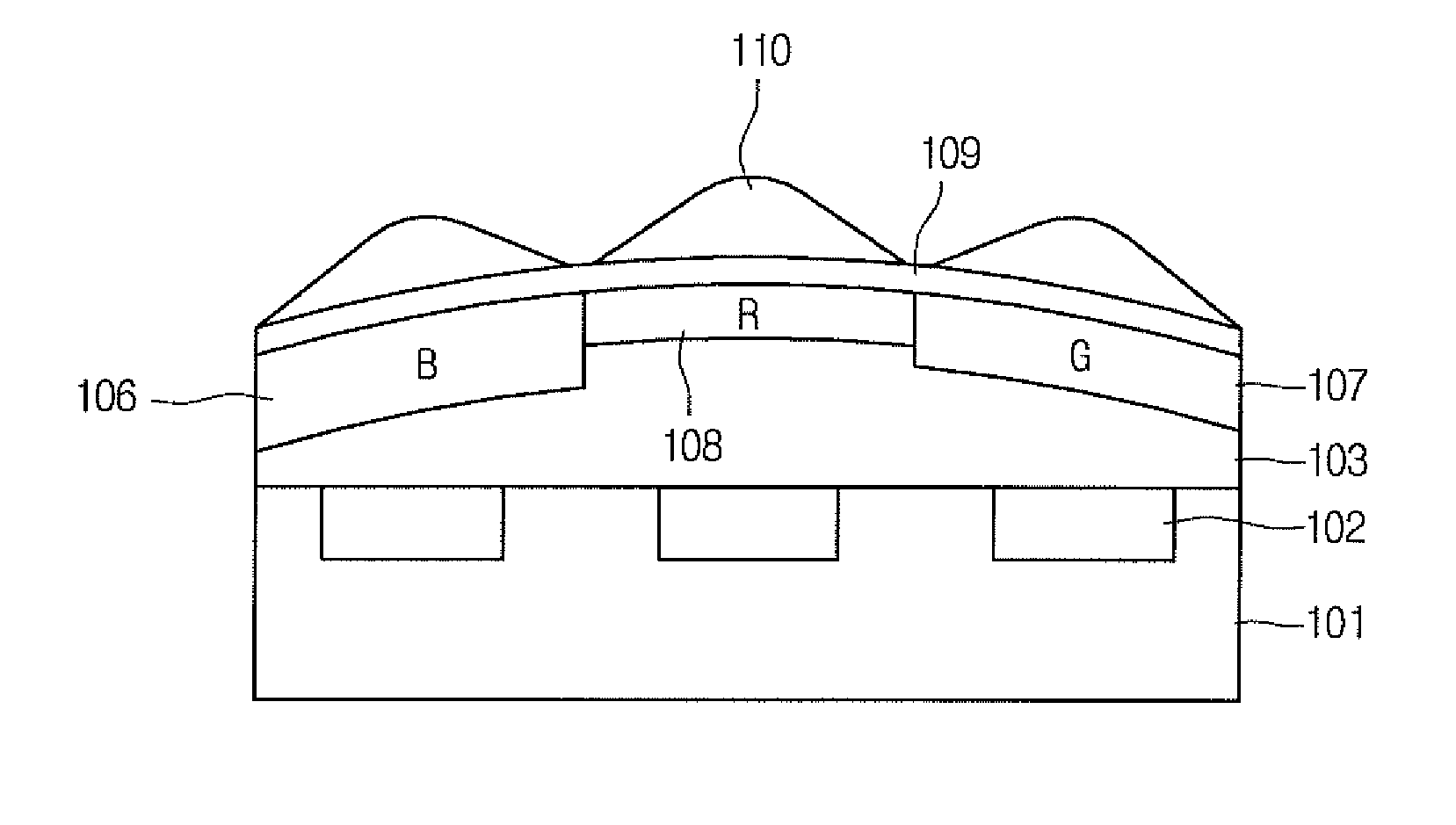
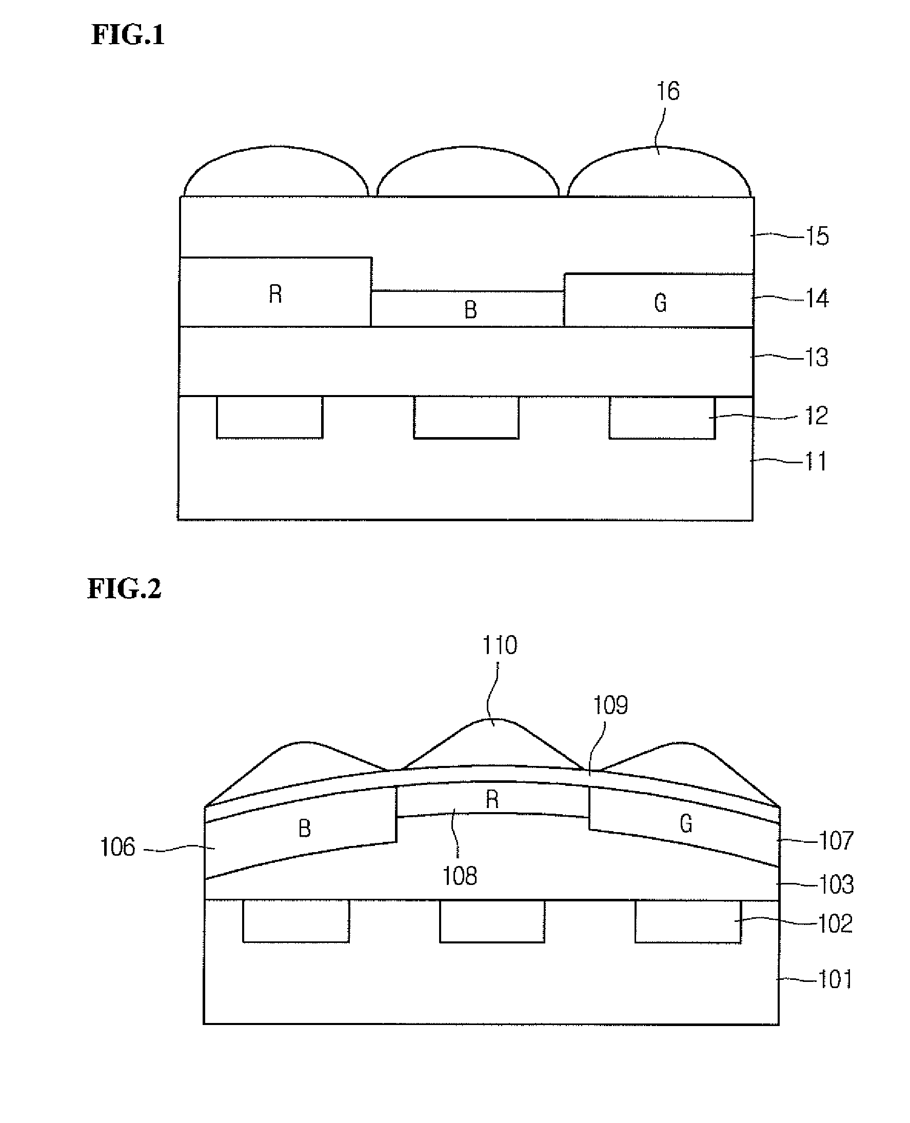
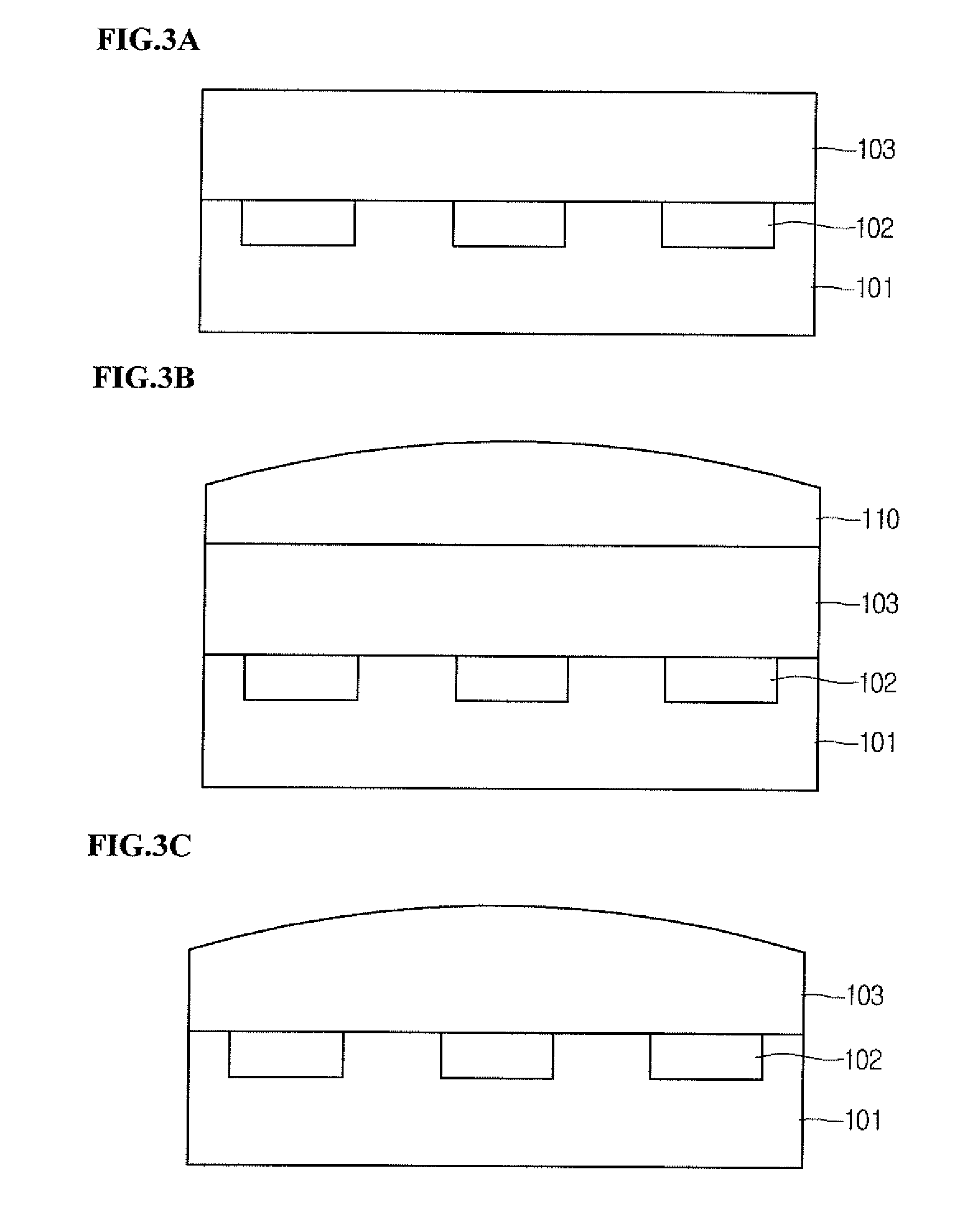
[0034]FIG. 2 is a cross-sectional view showing a CMOS image sensor according to an embodiment of the present invention.

[0035]Referring to FIG. 2, the CMOS image sensor can include at least one photodiode 102, a first planarization layer 103, a blue (B) color filter layer 106, a green (G) color filter layer 107, a red (R) color filter layer 108, a second planarization layer 109, and microlenses 110. The at least one photodiode 102 can be formed on a semiconductor substrate 101, and generates a charge according to an amount ...


PUM


Abstract

A CMOS image sensor and method of manufacturing same is provided. The CMOS image sensor can include: photodiodes formed on a semiconductor substrate for generating a charge according to an amount of incident light; a first planarization layer formed on the semiconductor substrate; a plurality of color filter layers formed on the first planarization layer, an upper surface of each of the color filter layers being curved; and a plurality of microlenses formed on the plurality of color filter layers.

Description

RELATED APPLICATION(S)[0001]This application claims priority under 35 U.S.C. §119(e) of Korean Patent Application No. 10-2005-0132638 filed Dec. 28, 2005, which is incorporated herein by reference in its entirety.FIELD OF THE INVENTION[0002]The present invention relates to an image sensor and a manufacturing method thereof.BACKGROUND OF THE INVENTION[0003]In general, image sensors are semiconductor devices that transform an optical image to electrical signals. Image sensors are generally classified as charge coupled device (CCD) image sensors or complementary metal oxide semiconductor (CMOS) image sensors.[0004]The CMOS image sensor includes a photodiode for sensing irradiated light and a CMOS logic circuit for generating data by processing the detected light into electric signals. As the amount of light received in the photodiode increases, the photosensitivity of the image sensor improves.[0005]In order to increase the photosensitivity of an image sensor, one method is to increase...

Claims


Application Information

Patent Timeline
Patent Type & Authority Applications(United States)
IPC IPC(8): H01L27/148
CPCH01L27/14621H01L27/14627H01L27/14632H01L27/14645H01L27/14685H01L27/14687H01L27/146
Inventor PARK, DONG BIN
Owner DONGBU ELECTRONICS CO LTD
Why Eureka
Try Eureka