

Modular probe card
- Summary
- Abstract
- Description
- Claims
- Application Information
AI Technical Summary
Benefits of technology
Problems solved by technology
Method used
Image

Examples
Embodiment Construction
[0013] Please refer to the attached drawings, the present invention will be described by means of embodiment(s) below.
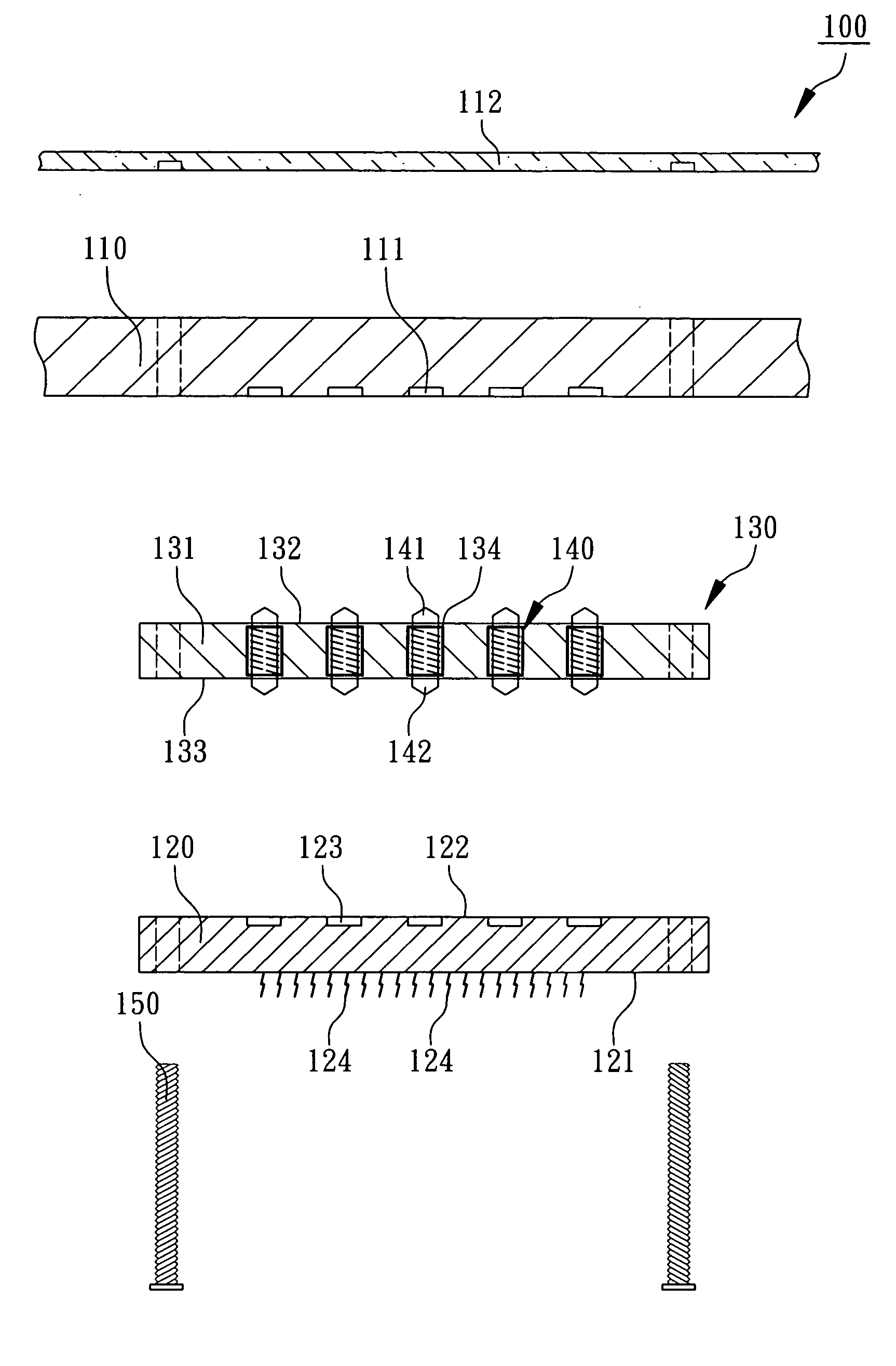
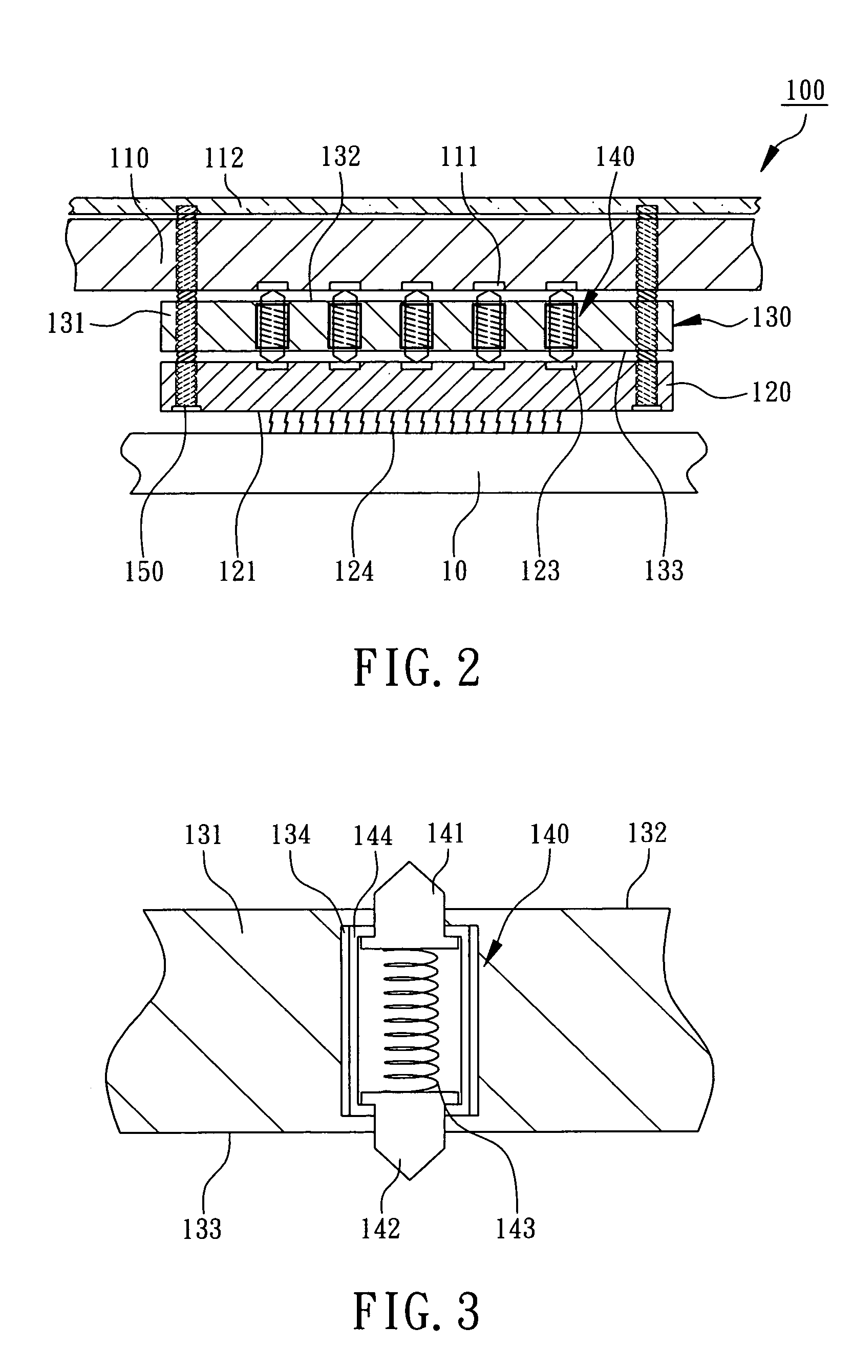
[0014] According to the embodiment of the present invention, a modular probe card is illustrated as shown in FIG. 1 and FIG. 2. The modular probe card 100 comprises a printed circuit board 110, a probe head 120, and an interposer 130 where the printed circuit board 110 has a plurality of first contact pads 111, and the probe head 120 has a plurality of second contact pads 123. The printed circuit board 110 is made from FR-4, FR-5, or BT resin with a multi-layer circuit design for mounting to a test head of an IC tester. The probe head 120 has a contact surface 121 and a joint surface 122 where a plurality of probes 124 are formed on the contact surface 121 such as vertical MEMS probes or elastic probes to probe a wafer 10 under test (as shown in FIG. 2), or other integrated circuits such as tape carrier packages (TCP), or chip-on-film packages (COF). The second cont...
PUM
 Abstract
Description
Claims
Application Information