

Non-volatile memory device having a nitride barrier to reduce the fast erase effect
Active Publication Date: 2007-07-05
MACRONIX INT CO LTD
View PDF4 Cites 4 Cited by
- Summary
- Abstract
- Description
- Claims
- Application Information
AI Technical Summary
Benefits of technology
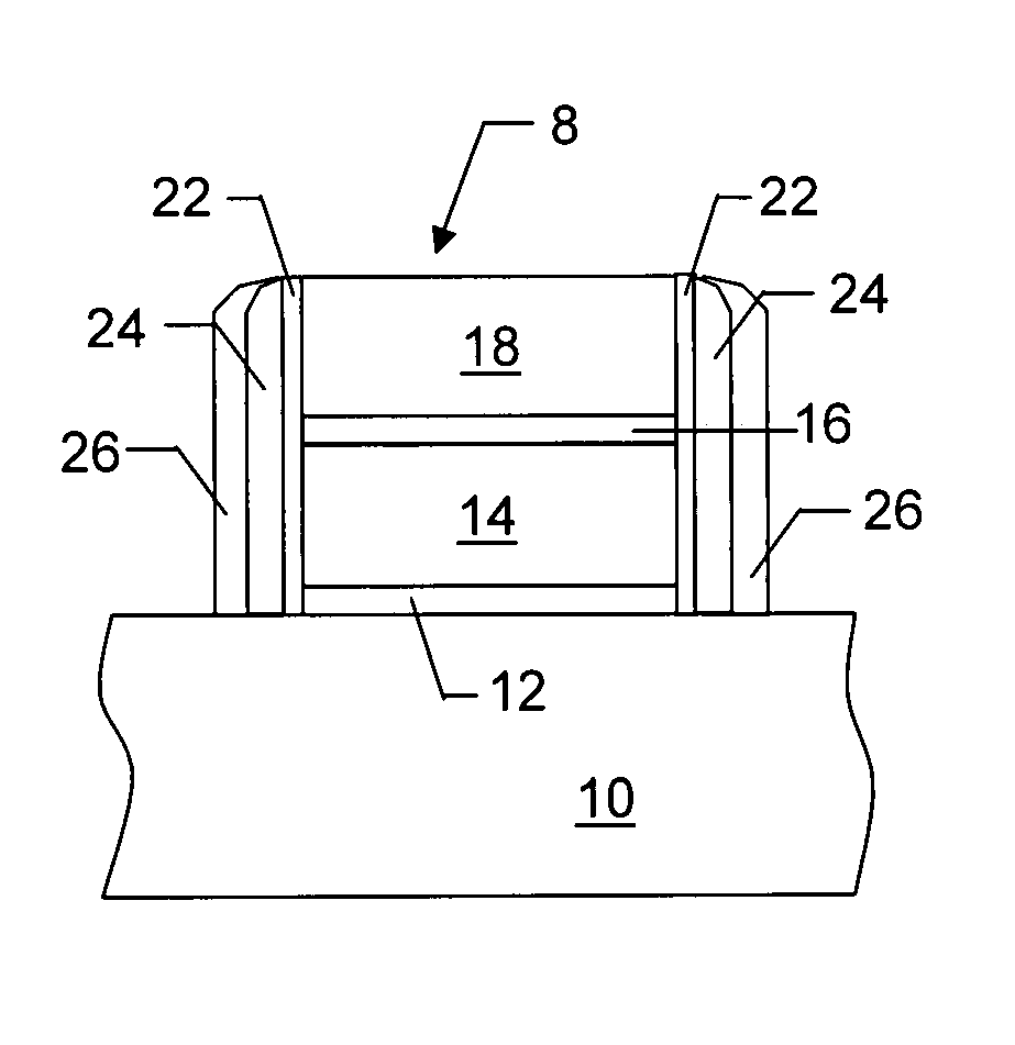
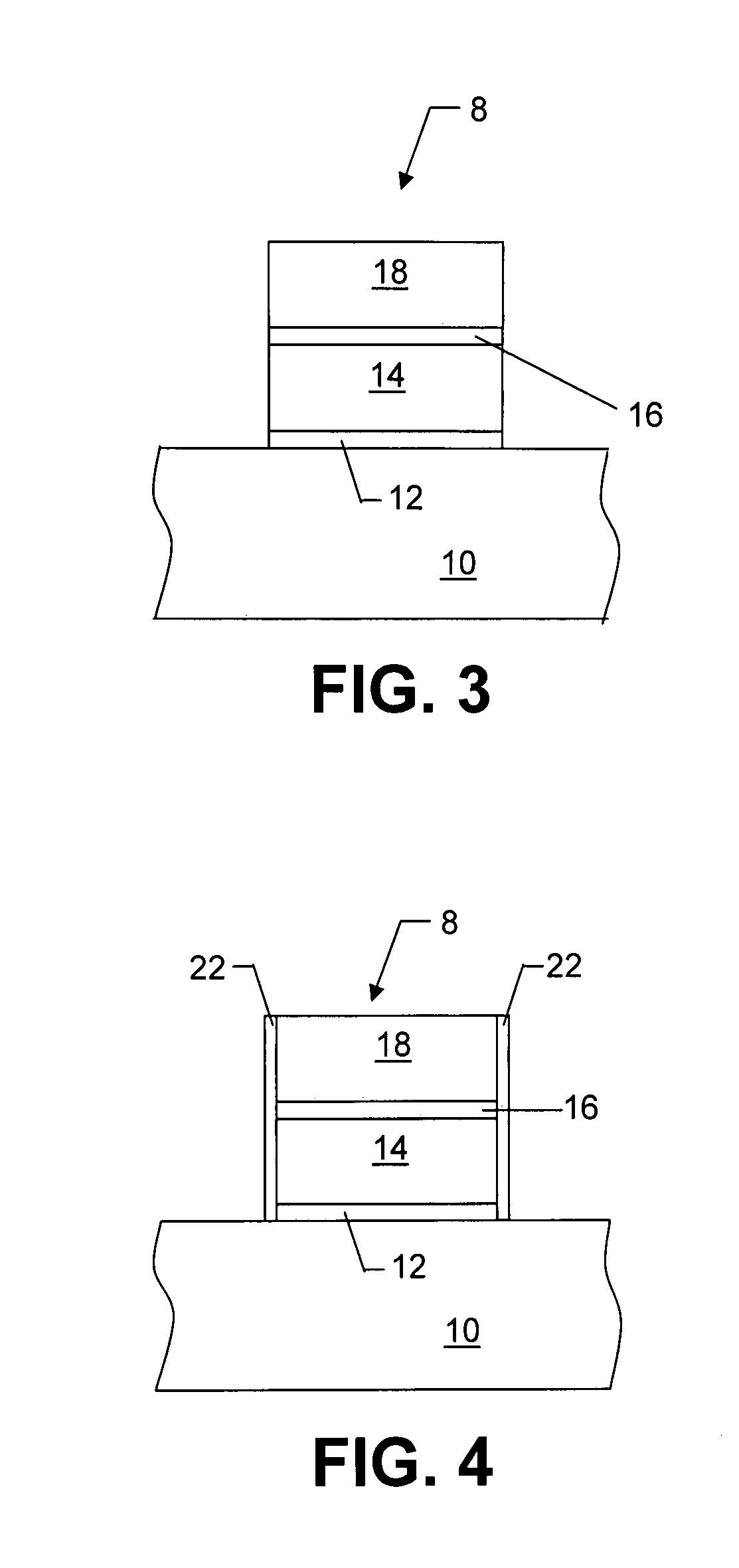
[0009] The present invention addresses these needs by providing a method for reducing the abnormal fast erase effect. In particular, a nitride (i.e., silicon nitride) barrier layer is formed laterally adjacent to the sidewalls of the stacked gate structure of a memory device. Because the nitride layer has the ability to trap negative charge, the nitride layer acts as a relatively high barrier at the tunneling oxide edge. Therefore, the threshold voltage difference between the initial erase and the erase after many cycles is reduced.
[0012] In the present invention, the presence of the nitride barrier layer provides protection against the fast erase effect by reducing or eliminating current leakage of the memory device. The nitride barrier layer tends to trap negative charge, particularly at the interface between the liner oxide layer and the nitride barrier layer. As such, the nitride barrier layer is strategically placed in the pathway of electrons that could otherwise pass from the floating gate to the source / drain regions. The nitride barrier layer thus forms a “barrier” that traps the electrons before they can reach the source / drain regions, thereby preventing current leakage. In the absence of current leakage, the difference between the memory cell's initial erase and the erase after many cycles is reduced such that the fast erase effect is attenuated or no longer a problem.
Problems solved by technology
In particular, the threshold voltage of the faster-erasing memory cells may be undesirably lower than the threshold voltage of other memory cells.
The faster-erasing memory cells thus may overerase, causing current leakage.
Excessive leakage currents can have adverse effects on the operation of the flash memory cell.
For example, the leakage currents of multiple cells in a column have a summing effect of leakage current on the bit-line and may result in an incorrect data reading.
Method used
View moreImage
Smart ImageViewing Examples

Examples
example
[0036] Several samples of a non-volatile memory device having a 200 Å nitride barrier layer were formed in accordance with the present invention. Samples of a conventional non-volatile memory device were also formed for comparison purposes. All samples were then subjected to 100 cycles of programming and erasing. The threshold voltage difference between the initial erase and the erase after 100 cycles was determined for each sample. FIG. 7 depicts a plot of the voltage differences for the conventional samples 30 and the samples 32 of the present invention. Conventional samples 30 exhibited voltage differences that are much greater than those exhibited by samples 32.
Login to View More PUM
 Abstract
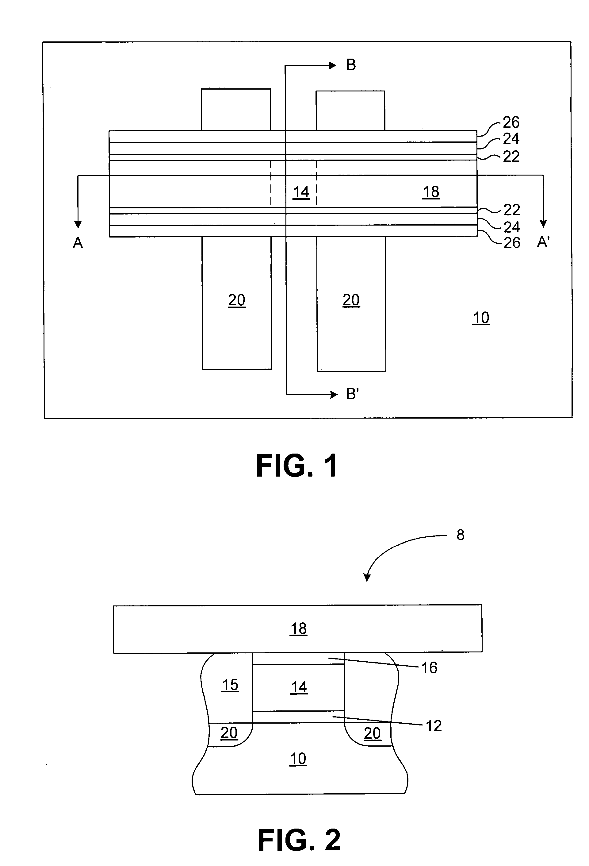
A method is provided for forming a non-volatile memory device. The method includes forming a stacked structure including a tunnel oxide layer, a floating gate, a thin oxide layer, and a control gate on a semiconductor substrate. Etching is used to define the sidewalls of the stacked structure. Dopants are implanted into exposed areas of the substrate to form source and drain regions within the substrate adjacent to the stacked structure. A liner dielectric layer is formed on the sidewalls of the stacked structure to patch the etching damage. Thereafter, a nitride barrier layer is formed on the liner dielectric layer, and an oxide spacer is formed on the nitride barrier layer. The nitride barrier layer can trap negative charge and thus act as a relatively high barrier at the tunneling oxide edge. Therefore, the threshold voltage difference between the initial erase of the memory device and the erase after many cycles is reduced.
Description
CROSS-REFERENCE TO RELATED APPLICATIONS [0001] This application is a divisional of U.S. Application Number 10 / 806,052, filed Mar. 22, 2004, the entire contents of which are hereby incorporated by reference.BACKGROUND OF THE INVENTION [0002] 1. Field of the Invention [0003] The present invention relates generally to semiconductor fabrication methods and, more particularly, to methods for fabricating a non-volatile memory device having a silicon nitride barrier layer to reduce the fast erase effect. [0004] 2. Description of Related Art [0005] Semiconductor devices typically include multiple individual components formed on or within a substrate. One such component is a memory device, which is used to store electronic data such as computer programs executed by an electronic processor and logical data operated on by the processor. Memory devices that do not require ambient power to store electronic data are commonly referred to as non-volatile memory devices. Flash memory is a specific f...
Claims
Login to View More Application Information
Patent Timeline
 IPC IPC(8): H01L21/336
CPCH01L29/2003H01L29/7881H01L29/66825H01L29/42324
InventorTSENG, UWAYLU, WENPINSU, CHUN-LIEN
OwnerMACRONIX INT CO LTD