Semiconductor device and manufacturing method of the semiconductor device

a semiconductor device and semiconductor technology, applied in the direction of semiconductor devices, basic electric elements, electrical appliances, etc., can solve the problems of abrupt reduction of the breakdown voltage of the semiconductor device, the reduction of the breakdown voltage of etc., to achieve the reduction of the electric field strength in the junction layer in the vicinity of the second conductivity type channel region, the effect of enhancing the breakdown voltage of the semiconductor device and reducing the breakdown voltag

Active Publication Date: 2007-07-12
FUJI ELECTRIC HLDG CO LTD
View PDF3 Cites 18 Cited by
  • Summary
  • Abstract
  • Description
  • Claims
  • Application Information

AI Technical Summary

Benefits of technology

[0041] According to the first aspect of the invention, the electric field strength in the junction layer in the vicinity of the second conductivity type channel region can be reduced. This can enhance the breakdown voltage of the semiconductor device and, at the same time, can reduce the on-voltage of the semiconductor device.
[0042] According to the second aspect of the invention, the electric field strength at the bottom of the trench in the junction layer can be reduced. This can enhance the breakdown voltage of the semiconductor device and, at the same time, can reduce the on-voltage of the semiconductor device.
[0043] According to the third to the eleventh aspects of the invention, the electric field strength in the junction layer in the vicinity of the second conductivity type channel region can be reduced.
[0046] According to the fourteenth aspect or the fifteenth aspect of the invention, the breakdown voltage of the semiconductor device can be enhanced and, at the same time, the on-voltage of the semiconductor device can be reduced.
[0047] According to the sixteenth aspect of the invention, the electric field strength in the junction layer in the vicinity of the second conductivity type channel region can be reduced. Thus, the breakdown voltage of the semiconductor device can be enhanced and, at the same time, the on-voltage of the semiconductor device can be reduced.
[0048] By the semiconductor device and the method of manufacturing the semiconductor device according to the invention, an effect is achieved that can raise a breakdown voltage as a characteristic at turning-off by weakening the electric field strength at the bottom of a trench, and at the same time, can lower the on-voltage as a characteristic in a turned-on state.

Problems solved by technology

This causes a reduction in a breakdown voltage, which is due to an unbalanced amount between the amount of impurity in the p RESURF layer and the amount of impurity in an n drift layer, smaller than that in a previous device.
The enhanced breakdown voltage, however, caused an accompanying problem of abruptly raising the on-voltage of the semiconductor device, and the measure for lowering the on-voltage caused a problem of abruptly reducing the breakdown voltage of the semiconductor device.

Method used


Image

  • Semiconductor device and manufacturing method of the semiconductor device
  • Semiconductor device and manufacturing method of the semiconductor device
  • Semiconductor device and manufacturing method of the semiconductor device

Examples


embodiment 1

Arrangement of the Semiconductor Device

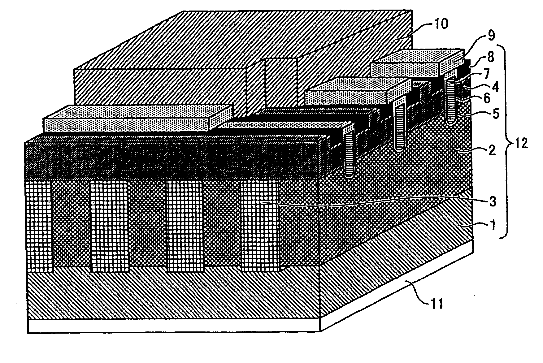
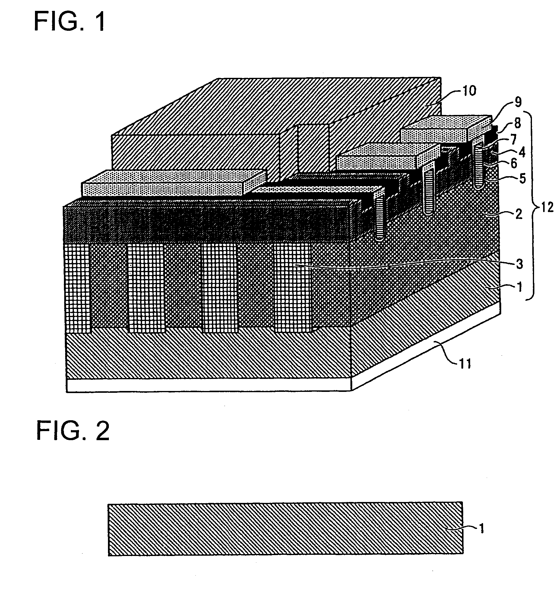
[0079]FIG. 1 is a perspective view showing an example of an arrangement of a semiconductor device according to Embodiment 1 of the invention. In Embodiment 1 a superjunction MOSFET with a breakdown voltage of 600 V is shown as an example of a vertical trench gate MOS power device. In the following description, the first conductivity type is n-type and the second conductivity type is p-type.

[0080] In FIG. 1, n-type drift regions 2 (first conductivity type semiconductor regions) and p-type partition regions 3 (second conductivity type semiconductor regions) are alternately provided to be aligned side by side on one of principal surfaces of n-type semiconductor substrate 1. N-type drift regions 2 and p-type partition regions 3 form a superjunction layer. On the superjunction layer, a p-type channel region 4 is formed. P-type channel region 4 has trenches 5 formed from the surface, each of which reaches the superjunction layer.

[0081] The bottom...

embodiment 2

[0094] Next, a method of manufacturing the semiconductor device according to Embodiment 2 will be explained. In Embodiment 1, the whole drift layer in between p-type channel region 4 and the n-type semiconductor substrate was provided as the superjunction layer. Embodiment 2, however, differs from Embodiment 1 in that a part of the drift layer is provided as the superjunction layer.

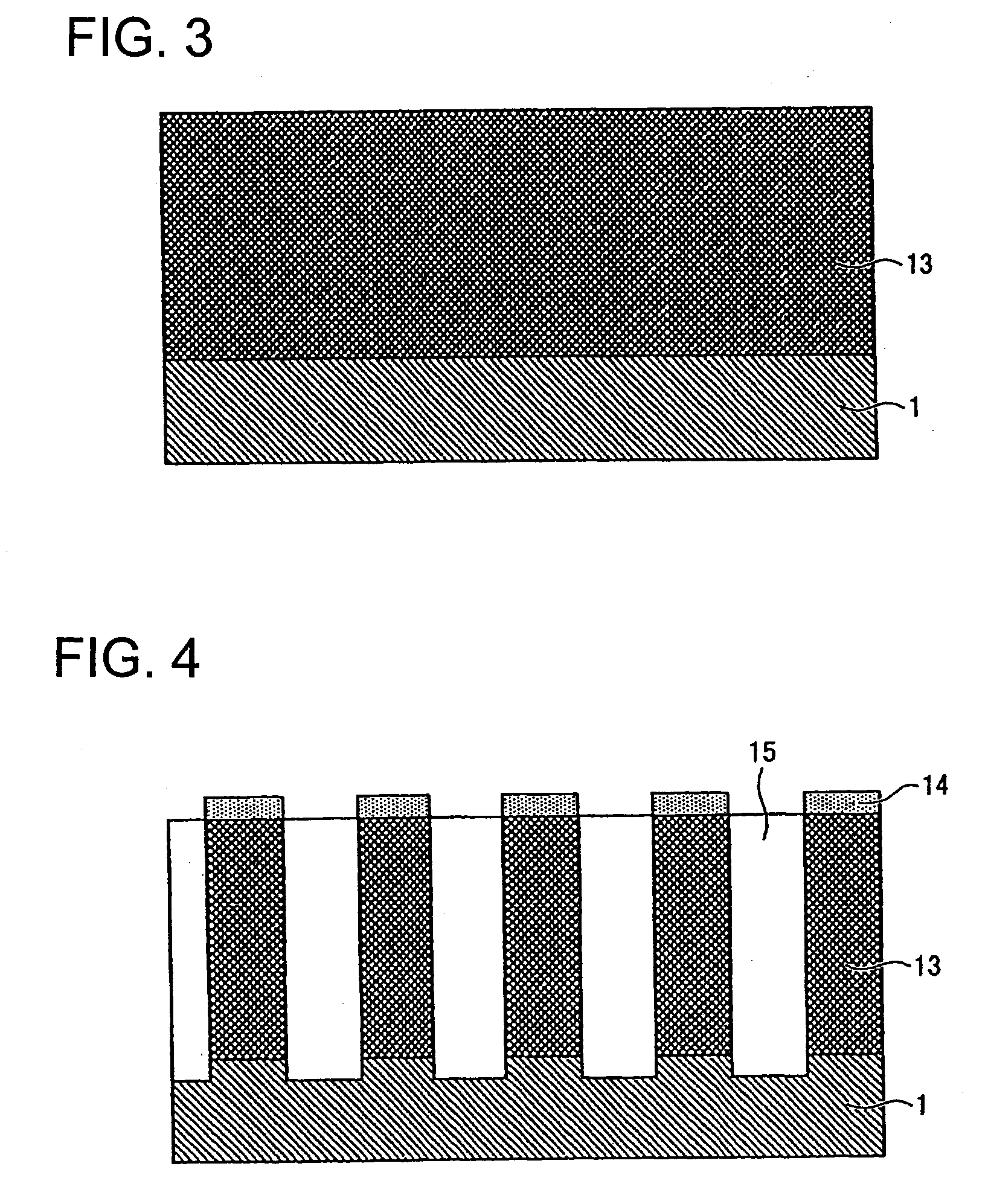
[0095] FIGS. 8 to 13 are cross sectional views showing arrangements in the steps of manufacturing the semiconductor device according to Embodiment 2. First, as shown in FIG. 8, an n-type semiconductor substrate 21 is prepared with the direction of crystal plane taken as (100) and an impurity concentration which is sufficiently high.

[0096] Then, as shown in FIG. 9, n-type silicon layer 22 with a concentration of impurities such as phosphorus atoms, for example, being on the order of 1.0×1015 cm−3, is epitaxially grown on n-type semiconductor substrate 21. Next to this, as shown in FIG. 10, n-type silicon...

embodiment 3

[0109] Next, a method of manufacturing the semiconductor device according to Embodiment 3 will be explained. In Embodiment 1, the junction plane of the n-type drift region 2 and the p-type partition region 3 was formed at approximately 90° to the p-type channel region 4. Embodiment 3, however, differs from Embodiment 1 in that the junction plane is formed at approximately 89° to the p-type channel region.

[0110] FIGS. 14 to 18 are cross sectional views showing arrangements in the steps of manufacturing the semiconductor device according to Embodiment 3. First, as shown in FIG. 14, n-type semiconductor substrate 31 is prepared with the direction of crystal plane taken as (100) and an impurity concentration which is sufficiently high.

[0111] Then, as shown in FIG. 15, p-type silicon layer 32 with a concentration of impurities such as boron atoms, for example, being on the order of 4.46×1015 cm−3, is epitaxially grown on n-type semiconductor substrate 31 to a thickness of approximately...


PUM


Abstract

A semiconductor device including an n-type semiconductor substrate, a p-type channel region and a junction layer provided between the n-type semiconductor substrate and the p-type channel region is disclosed. The junction layer has n-type drift regions and p-type partition regions alternately arranged in the direction in parallel with the principal surface of the n-type semiconductor substrate. The p-type partition region forming the junction layer is made to have a higher impurity concentration than the n-type drift region. This enables the semiconductor device to have an enhanced breakdown voltage and, at the same time, have a reduced on-resistance.

Description

CROSS REFERENCE TO RELATED APPLICATIONS [0001] This application claims priority from Japanese application serial no. 2005-342587, filed on Nov. 28, 2005, the contents of which are incorporated herein in their entirety. BACKGROUND OF THE INVENTION A. Field of the Invention [0002] The present invention relates to a high-power vertical insulated gate semiconductor device, and in more detail, to a trench gate superjunction semiconductor device having a trench gate, which has a trench, an insulator film formed therein and a control electrode filling the trench with the insulator film held between, and having a superjunction layer in a semiconductor substrate. B. Description of the Related Art [0003] In recent years, in compliance with requirements for downsizing and performance enhancement in power source equipment in the field of power electronics, efforts have been concentrated on a power semiconductor device to improve the performance in obtaining a high breakdown voltage, a high cu...

Claims


Application Information

Patent Timeline
Patent Type & Authority Applications(United States)
IPC IPC(8): H01L29/94H01L21/336
CPCH01L29/0634H01L29/0878H01L29/1095H01L29/402H01L29/7813H01L29/4236H01L29/66734H01L29/7802H01L29/7811H01L29/41741
Inventor YOSHIKAWA, KOHSUGI, AKIOTAKAHASHI, KOUTATAKEI, MANABUNAKAZAWA, HARUOIWAMURO, NORIYUKI
Owner FUJI ELECTRIC HLDG CO LTD
Why Eureka
Try Eureka