Semiconductor device

a technology of semiconductor devices and semiconductor chips, applied in the direction of electrical transducers, loudspeakers, microphone structural associations, etc., can solve the problems of reducing the accuracy of pressure variation detection, difficult to downsize the semiconductor device, and large overall size of the substrate, so as to avoid the occurrence of operational errors, prevent electromagnetic noise, and establish the precise positioning of the circuit chip relative to the stage with eas

Inactive Publication Date: 2007-07-12
YAMAHA CORP
View PDF1 Cites 83 Cited by
  • Summary
  • Abstract
  • Description
  • Claims
  • Application Information

AI Technical Summary

Benefits of technology

[0011] It is an object of the present invention to provide a semiconductor device that can be downsized with ease.
[0012] It is another object of the present invention to provide a semiconductor device and a manufacturing method therefor, in which an electromagnetic shield embracing a semiconductor chip and a circuit chip can be formed with ease.

Problems solved by technology

This reduces the displacement of the diaphragm, thus reducing the accuracy of the detection of pressure variations.
Due to the parallel arrangement of the semiconductor chip and the circuit chip, which are attached onto the surface of the substrate, the overall size of the substrate becomes large; hence, it is difficult to downsize the semiconductor device.
In the above, the conductive layer of the substrate needs to be designed so as not to cause interference with electronic circuits and wirings of the semiconductor chip and circuit chip; and this is troublesome in circuit designing.

Method used


Image

  • Semiconductor device
  • Semiconductor device
  • Semiconductor device

Examples


first embodiment

1. First Embodiment

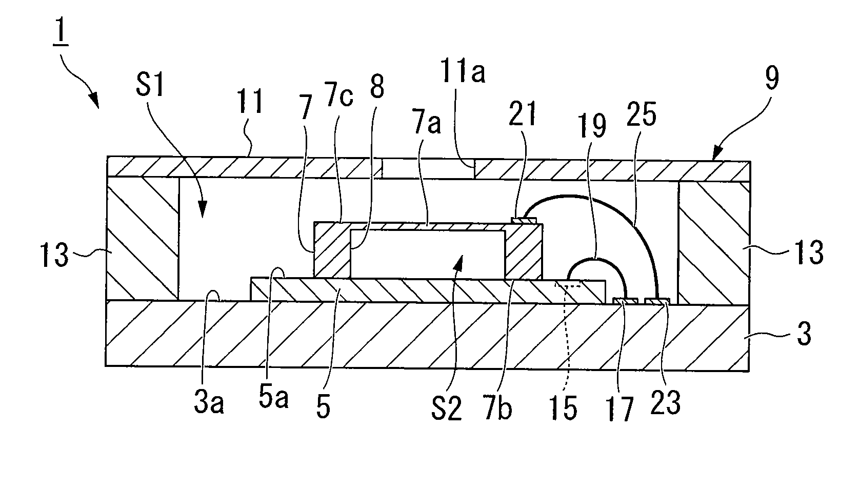
[0068]FIG. 1 is a cross-sectional view showing the internal structure of a semiconductor device 1 in accordance with a first embodiment of the present invention. The semiconductor device 1 includes a circuit chip (hereinafter, referred to as an LSI chip) 5 and a semiconductor chip 7, which are sequentially formed on a surface 3a of a substrate 3. In addition, a cover member 9 is arranged so as to entirely cover the LSI chip 5 and the semiconductor chip 7 on the surface 3a of the substrate 3.

[0069] The substrate 3 is designed as a multilayered wiring substrate having electrical wirings (not shown), which establish electrical connection with the LSI chip 5 and the semiconductor chip 7.

[0070] The cover member 9 has a top portion 11 having a rectangular shape, which is positioned above the surface 3a of the substrate 3, and side walls 13, which are arranged in a ring shape and are fixed to the periphery of the surface 3a of the substrate 3. The cover member 9 as a w...

second embodiment

2. Second Embodiment

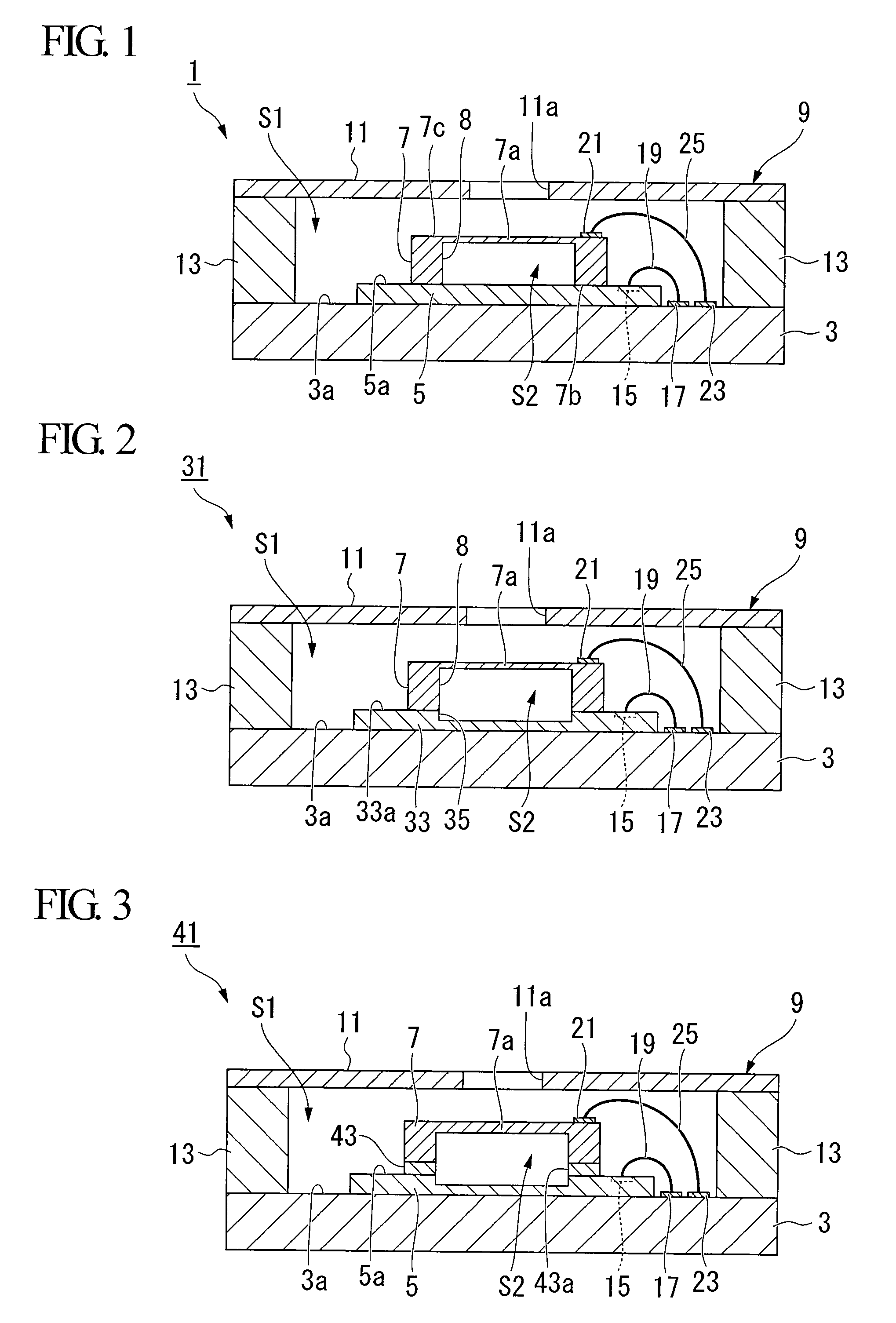
[0122] A second embodiment of the present invention will be described in detail with reference to FIG. 10, FIGS. 11A-11D, FIG. 12, and FIG. 13. A semiconductor device 201 of the second embodiment is mounted on a substrate (or a printed-circuit board) 203 and is constituted of an LSI chip (or a circuit chip) 205 mounted on a surface 203a of the substrate 203, a silicon capacitor microphone chip (or a semiconductor chip) 207 attached onto a surface 205a of the LSI chip 205, and a cover member 209 for covering the LSI chip 205 and the silicon capacitor microphone chip 207. Herein, both of the LSI chip 205 and the silicon capacitor microphone chip 207 are formed in substantially the same size. That is, when the LSI chip 205 and the silicon capacitor microphone chip 207 are vertically combined together, the silicon capacitor microphone chip 207 does not horizontally extend out of the LSI chip 205 in plan view.

[0123] A plurality of electrodes 211 are formed so as to r...

third embodiment

3. Third Embodiment

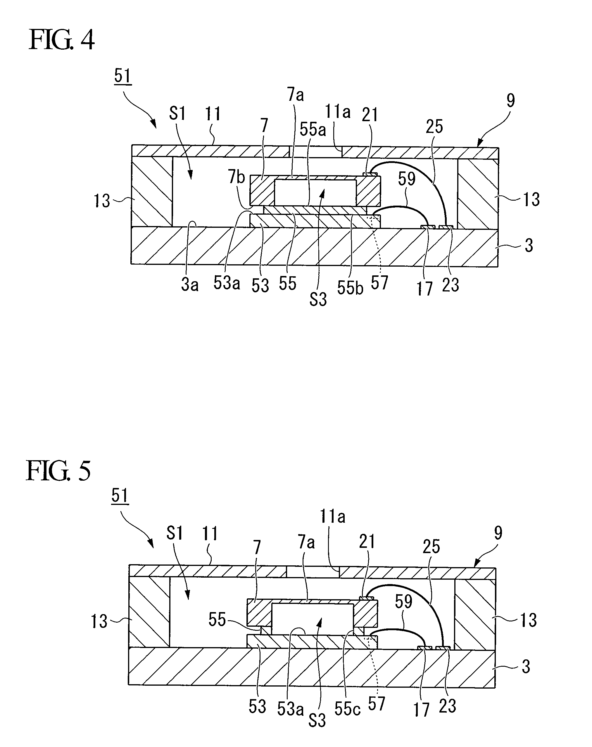
[0172] With reference to FIG. 14, FIGS. 15A-15E, and FIGS. 16-17, and FIGS. 18A and 18B, a semiconductor device 301 will be described in accordance with a third embodiment of the present invention. The semiconductor device 301, which is mounted on a substrate (or a printed-circuit board, not shown), is designed to include an LSI chip (or a circuit chip) 303, a silicon capacitor microphone chip (or a semiconductor chip) 305, which is attached onto a surface 303a of the LSI chip 303 and is electrically connected together with the LSI chip 303, and a shield case 307 for embracing the LSI chip 303 and the silicon capacitor microphone chip 305 therein. Both of the LSI chip 303 and the silicon capacitor microphone chip 305 are the same size in plan view. That is, when the silicon capacitor microphone chip 305 is vertically combined with the LSI chip 303, the side portions of the silicon capacitor microphone chip 305 do not extend from the side portions of the LSI chip 3...


PUM


Abstract

A semiconductor device includes a substrate, a semiconductor chip having a diaphragm, which vibrates in response to sound pressure variations, and a circuit chip that is electrically connected to the semiconductor chip so as to control the semiconductor chip, wherein the semiconductor chip is fixed to the surface of the circuit chip whose backside is mounted on the surface of the substrate. Herein, a plurality of connection terminals formed on the backside of the semiconductor chip are electrically connected to a plurality of electrodes running through the circuit chip. A ring-shaped resin sheet is inserted between the semiconductor chip and the circuit chip. The semiconductor chip and the circuit chip vertically joined together are stored in a shield case having a mount member (e.g., a stage) and a cover member, wherein connection terminals of the circuit chip are exposed to the exterior via through holes of the stage.

Description

BACKGROUND OF THE INVENTION [0001] 1. Field of the Invention [0002] The present invention relates to semiconductor devices having semiconductor chips such as pressure sensor chips and sound pressure sensor chips. [0003] This application claims priority on Japanese Patent Applications Nos. 2005-375837, 2006-87942, and 2006-172617, the contents of which are incorporated herein by reference. [0004] 2. Description of the Related Art [0005] In semiconductor devices serving as silicon capacitor microphones and pressure sensors, semiconductor chips (e.g., pressure sensor chips and sound pressure sensor chips mounted on substrates) include diaphragms that vibrate in response to pressures applied thereto so as to detect pressure variations such as sound pressure variations. Japanese Patent Application Publication No. 2004-537182 discloses an example of a miniature silicon capacitor microphone. In this type of semiconductor device whose semiconductor chip is mounted on a substrate, a cavity i...

Claims


Application Information

Patent Timeline
Patent Type & Authority Applications(United States)
IPC IPC(8): H01L23/34
CPCB81B7/0064H01L2224/48091H01L2924/3025H01L2924/00014H01L2924/00H04R1/04H04R2201/003
Inventor SAKAKIBARA, SHINGOSAITOH, HIROSHI
Owner YAMAHA CORP
Why Eureka
Try Eureka