Antenna circuit, IC inlet, multi tag, and method for producing multi tag

a technology of ic inlet and multi-tag, which is applied in the field of nano circuit, multi-tag and multi-tag production method, can solve the problems of increasing the cost of ic tag, increasing the load of work, increasing the waste of tag, etc., and achieves the effect of efficient production

Inactive Publication Date: 2007-07-12
LINTEC CORP
View PDF4 Cites 21 Cited by
  • Summary
  • Abstract
  • Description
  • Claims
  • Application Information

AI Technical Summary

Benefits of technology

[0024]Thus, the plurality of circuit units can be formed on the circuit substrate. Therefore, neither the amount of the material nor the workload necessary for a conventional circuit manufacturing are changed by forming the small circuit unit with the same ...

Problems solved by technology

Therefore, since the cost of the IC tag increases in proportion to the number of sheets, and the same manufacturing of IC tags of data writing processing and surface print processing, etc. are necessary, the load of work also increases.
Moreover, there is a pro...

Method used


Image

  • Antenna circuit, IC inlet, multi tag, and method for producing multi tag
  • Antenna circuit, IC inlet, multi tag, and method for producing multi tag
  • Antenna circuit, IC inlet, multi tag, and method for producing multi tag

Examples


first embodiment

(A) First Embodiment

[0034]Hereafter, a first embodiment according to the present invention of an antenna circuit, an IC inlet, a multi tag, and a method for producing the multi tag will be explained referring to the drawing.

(A-1) Configuration of the First Embodiment

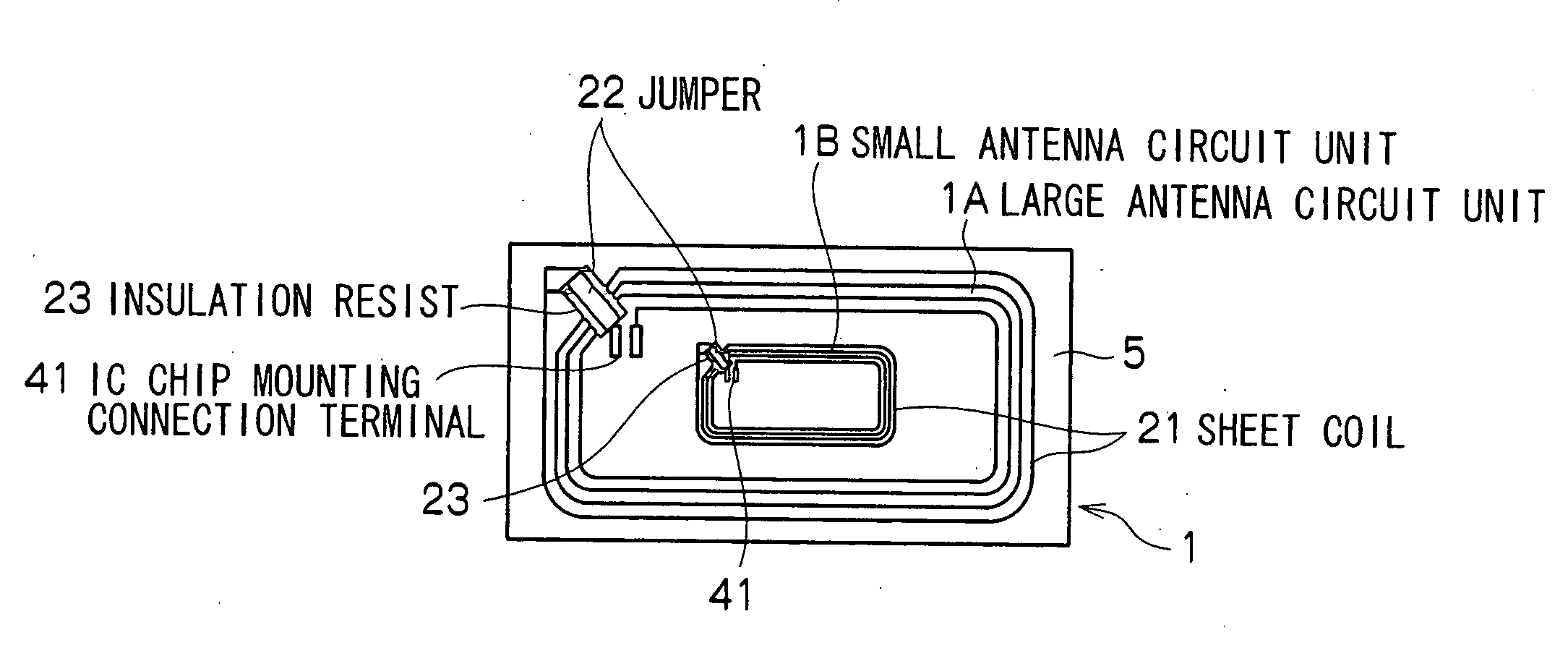
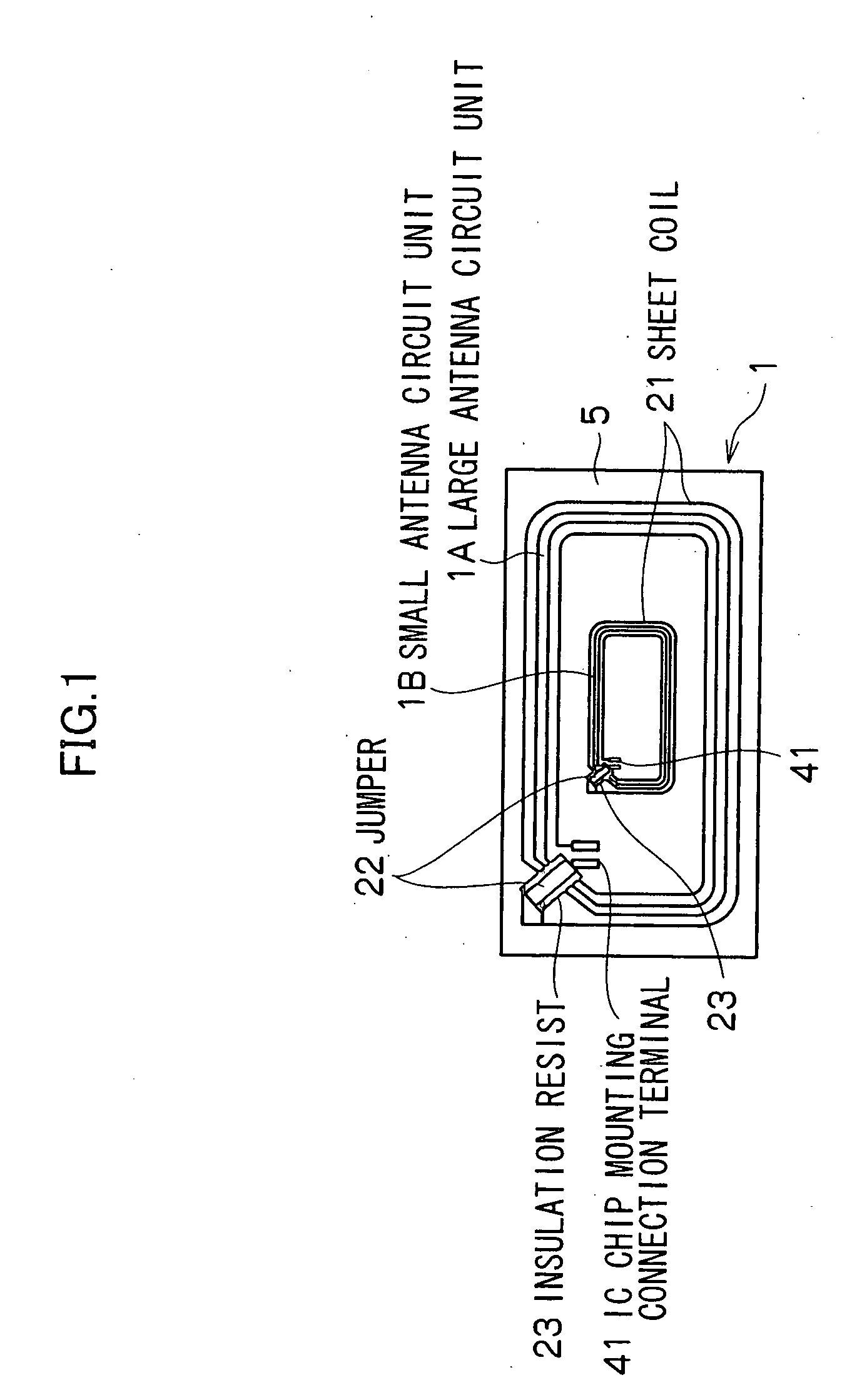
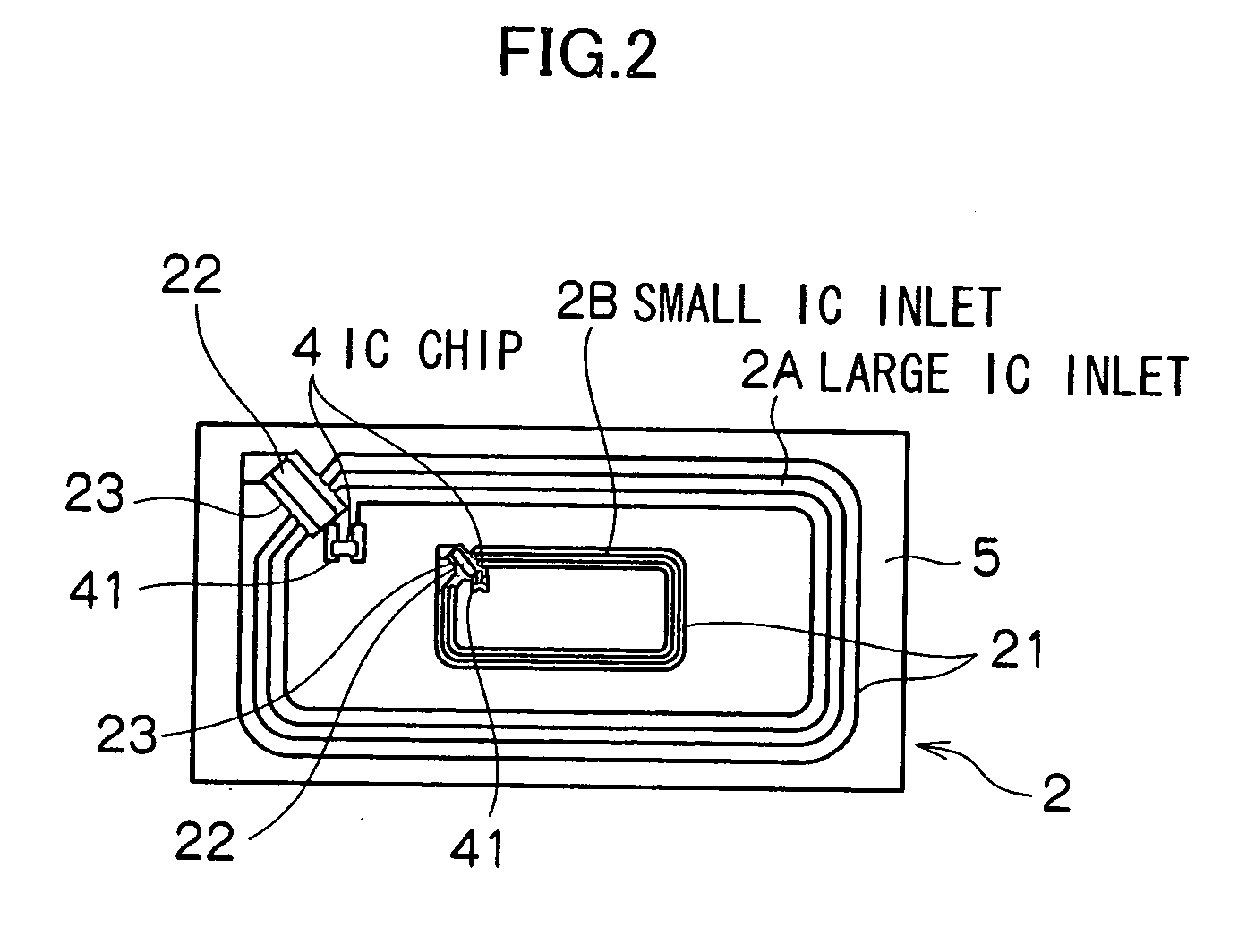
[0035]FIG. 1 is an illustration for explaining an example of configuring an antenna circuit according to the present embodiment, FIG. 2 is an illustration for explaining an example of configuring an IC inlet according to the present embodiment, and FIG. 3 shows an example of a shape of a multi tag by processing tag according to the present embodiment.

[0036]Here, the IC inlet indicates a circuit in the state of FIG. 2 where an IC chip 4 is mounted on an IC chip mounting connection terminal 41 of a large antenna circuit unit 1A and / or a small antenna circuit unit 1B in FIG. 1. Moreover, FIG. 3 shows a tag shape after processing tag, and the cross section configuration is shown in FIG. 4.

[0037]As shown in FIG. 1, in an ante...

example

[0089]Next, since the IC tag 3 of the first embodiment has been produced, the production method and the characteristic thereof will be explained.

[0090]First of all, a copper foil film laminate (NIKKAN INDUSTRIES Co., Ltd.: trade name “NIKAFLEX”) to which the copper foil (35 μm in thickness) is laminated in advance for a film of polyethylene terephthalate (PET) resin (50 μm in thickness) as the circuit substrate 5 was used.

[0091]An etching resist pattern was printed by a screen printing in order to form an antenna circuit to this copper foil surface. At this time, an outside size of the large antenna circuit unit 1A was set to 32 mm in length and 61 mm in width, and the sheet coil 21 was set to line width 200 μm, line spacing 400 μm, and 7 times of the turn number. On the other hand, an inside size of the small antenna circuit unit 1B was set to 16 mm in length and 22 mm in width, and the sheet coil 21 was set to line width 130 μm, line spacing 120 μm, and 14 times of the turn number...


PUM


Abstract

An antenna circuit includes a plurality of antenna circuit units on a circuit substrate. The plurality of antenna circuit units includes: a large antenna circuit unit whose circuit size is large; and a small antenna circuit unit whose circuit size is smaller than the size of the large antenna circuit unit, the small antenna circuit unit provided inside the large antenna circuit unit and provided detachable from the large antenna circuit unit.

Description

CROSS-REFERENCE TO RELATED APPLICATION[0001]This application claims, under 35 USC 119, priority of Japanese Application No. 2006-5179 filed Jan. 12, 2006.BACKGROUND OF THE INVENTION[0002]1. Field of the Invention[0003]The present invention relates to an antenna circuit, an IC inlet, a multi tag, and a method for producing the multi tag.[0004]2. Description of the Background Art[0005]Recently, an IC tag of non-contact type has been used in various processing of the personal identification, the merchandise control, the physical distribution management, and the theft measures, etc.[0006]For example, when used for the physical distribution management, one IC tag is attached to the article, and a confirmation machine (for example, reader / writer device etc.) can read or rewrite inside information of an IC chip that the IC tag mounts. As a result, it is possible to verify and manage information on the article of the actual thing by matching with management data in an upper level data base....

Claims


Application Information

Patent Timeline
IPC IPC(8): G08B13/14
CPCG06K19/07749H01Q1/24G06K19/077G06K19/07
Inventor MATSUURA, KATSUYOSHIKATAKURA, KATSUMIMATSUSHITA, TAIGA
Owner LINTEC CORP
Why Eureka
Try Eureka