Liquid crystal display and methods of fabricating and repairing the same

a technology of liquid crystal display and lcd, applied in the direction of liquid/fluent solid measurement, volume metering, instruments, etc., can solve the problems of reducing the rate of pixel repair, complicating the repairing process, and side visibility distortion phenomenon of conventional pva type lcd

Active Publication Date: 2007-07-12
SAMSUNG DISPLAY CO LTD
View PDF1 Cites 41 Cited by
  • Summary
  • Abstract
  • Description
  • Claims
  • Application Information

AI Technical Summary

Benefits of technology

[0033]At least any one of the first and second pixel patterns may include a aperture pattern, and the cut connection terminal may be cut in the aperture pattern between the first and second pixel patterns.
[0034]A laser beam may be radiated onto an overlapped region of the uncut connection terminal with the repair line and an overlapped region of the repair electrode with the repair line, so that the uncut connection terminal, the repair line and the repair electrode in the overlapped region can be connected to one another. A laser beam may be radiated onto an overlapped region of the cut connection terminal with the repair line, so that the pixel pattern connected to the cut connection terminal can be connected to the repair line.
[0035]If a failure occurs in a region of the first switching element and the first pixel pattern overlaps with the repair electrode, the first connection terminal may be cut, the second connection terminal may be connected to the repair line, and the repair electrode may be connected to the repair line. If a failure occurs in a region of the second switching element and the first pixel pattern overlaps with the repair electrode, the second connection terminal may be cut, and the first and second connection terminals may be connected to the repair line.

Problems solved by technology

However, a side visibility distortion phenomenon occurs in the conventional PVA type LCD.
This complicates the repairing process and thus lowers the rate of a successful pixel repair.
However, since two pixel patterns are provided within the region of one pixel and two TFTs for respectively driving them are included in the structure, a channel failure generating rate of the TFTs due to contaminations is twice that of a case where one TFT is provided for one pixel pattern.
Further, the number of lines for use in driving a plurality of pixel patterns increases, and accordingly, a failure rate increases due to an increase in pattern density.

Method used


Image

  • Liquid crystal display and methods of fabricating and repairing the same
  • Liquid crystal display and methods of fabricating and repairing the same
  • Liquid crystal display and methods of fabricating and repairing the same

Examples


Embodiment Construction

[0054]Hereinafter, exemplary embodiments of the present invention will be described in detail with reference to the accompanying drawings. In the drawings, the thicknesses of layers and regions are exaggerated for clarity, and like reference numerals are used to designate like elements throughout the specification and drawings. Further, an expression that an element such as a layer, region, substrate or plate is placed on or above another element indicates not only a case where the element is placed directly on or just above the other element but also a case where a further element is interposed between the element and the other element.

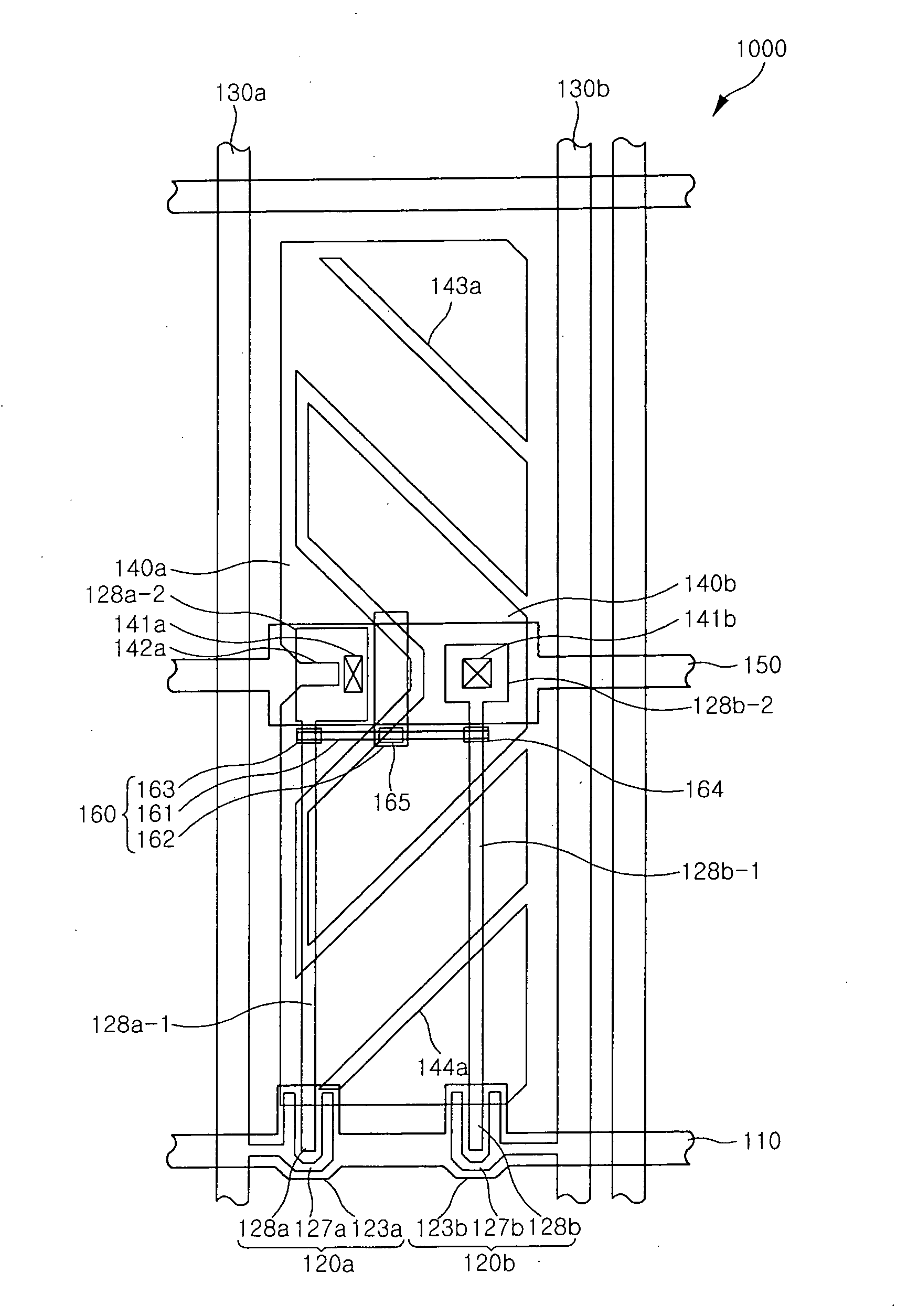
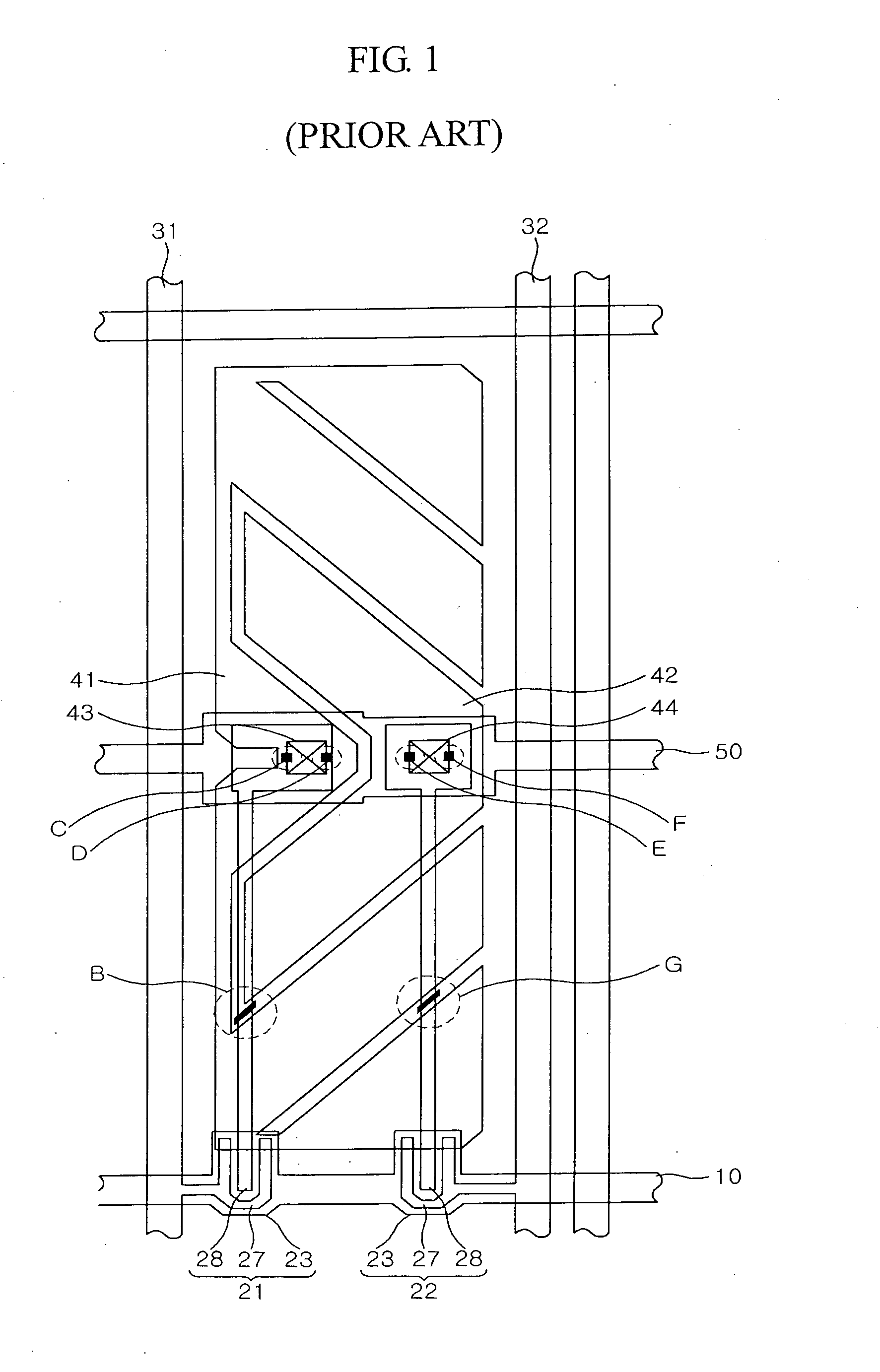
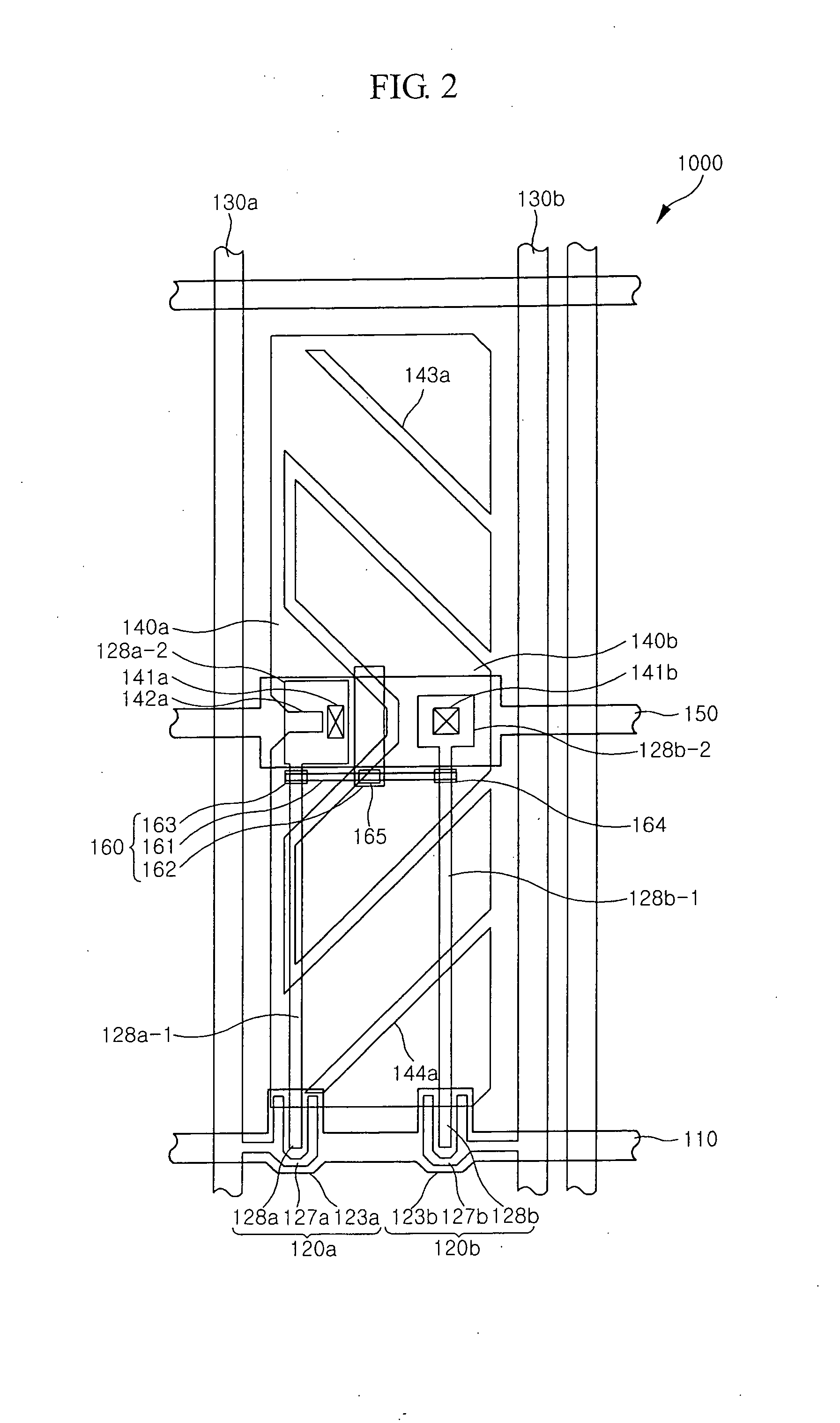
[0055]FIG. 2 is plan view of a thin film transistor (TFT) substrate according to an embodiment of the present invention. FIG. 3 is a plan view of a color filter substrate according to an exemplary embodiment of the present invention. FIG. 4 is a plan view of an LCD in which the TFT substrate of FIG. 2 and the color filter substrate of FIG. 3 are comb...


PUM

PropertyMeasurementUnit
voltageaaaaaaaaaa
sizeaaaaaaaaaa
weightaaaaaaaaaa

Abstract

A liquid crystal display comprising first and second switching elements connected to a first signal line; a signal line pair including a second and a third signal line connected to the first and second switching elements, respectively; a first pixel pattern connected through a first connection terminal of the first switching element; a second pixel pattern connected through a second connection terminal of the second switching element; a storage electrode line overlapping with the first and second pixel patterns; and a repair portion for electrically connecting the first and second pixel patterns to each other through a repairing process.

Description

CROSS-REFERENCE TO RELATED PATENT APPLICATION[0001]This application claims priority to Korean Patent Application No. 2006-0003234, filed on Jan. 11, 2006, in the Korean Intellectual Property Office, the disclosure of which is incorporated by reference herein.BACKGROUND OF THE INVENTION[0002]1. Technical Field[0003]The present disclosure relates to a liquid crystal display, and methods of fabricating and repairing the same, and more particularly, to a method of repairing a liquid crystal display with two sub-pixels in one pixel.[0004]2. Discussion of the Related Art[0005]Since a liquid crystal display (LCD) has advantages of small size, light weight and low power consumption as compared to a conventional cathode ray tube (CRT), the LCDs are widely favored over the CRTs.[0006]An LCD is a device in which two substrates with electrodes formed thereon are positioned such that the two electrodes face each other, a liquid crystal substance is injected between the two substrates, and an ele...

Claims


Application Information

Patent Timeline
Patent Type & Authority Applications(United States)
IPC IPC(8): G02F1/1333
CPCG02F2001/136268G02F1/136259G02F1/136268G01F15/005G01F15/10
Inventor YANG, BYUNG DUK
Owner SAMSUNG DISPLAY CO LTD
Why Eureka
Try Eureka