Stacked mounting structure

a mounting structure and stacked technology, applied in the direction of microstructural devices, printed circuit aspects, stacked spaced pcbs, etc., can solve the problems of high degree of difficulty in mounting, difficult to deal with automatic packaging machines, and the job of disposing and soldering, so as to reduce the projected area, reduce the size, and improve the yield

Active Publication Date: 2007-07-19
OLYMPUS CORP
View PDF2 Cites 14 Cited by
  • Summary
  • Abstract
  • Description
  • Claims
  • Application Information

AI Technical Summary

Benefits of technology

[0011] The present invention is made upon taking into consideration the problems mentioned above, and an object of the present invention is to provide a stacked mounting structure in which a plurality of substrates is connected via spacers, and components to be mounted are mounted in a space between the substrates, while reducing a size by decreasing a projected area in a direction of a plane of the substrate, and a method of manufacturing the stacked mounting structure in which, an improvement in a yield, a reduction in a cost, and a shortening of a manufacturing time are realized by decreasing number of steps in a manufacturing process.

Problems solved by technology

For example, a job of disposing and soldering short lead wires on a minute structure which is disposed three-dimensionally, is impossible to deal with in an automatic packaging machine.
Moreover, even with the job carried out manually, such mounting is categorized to be having a high degree of difficulty.
A technology in which the automation is difficult, and the degree of difficulty of the job is high, leads to an increase in a mounting cost and a decline in productivity.
Moreover, taking into consideration a size of the lead wire which can be handled in a manual job and a gap between the lead wires which can be controlled during the handling, a structure according to the conventional technology is not favorable for reducing a size of the mounting structure.
Therefore, it is difficult to narrow a pitch of a joining portion.
In other words, it is difficult to reduce a projected area when the structure is viewed from a top.
Therefore, there is a drawback that a resistance of the connecting portion between the electroconductive spacer 25 and the substrate 21 becomes high.
Thus, in the conventional mounting structure, it is difficult to ensure a favorable productivity for stacking a substrate via the spacer in order to ensure a mounting space of the electronic components.
Moreover, it is also difficult to reduce the size such that a projected area in a direction of a plane of the substrate is decreased.

Method used


Image

  • Stacked mounting structure
  • Stacked mounting structure
  • Stacked mounting structure

Examples


first embodiment

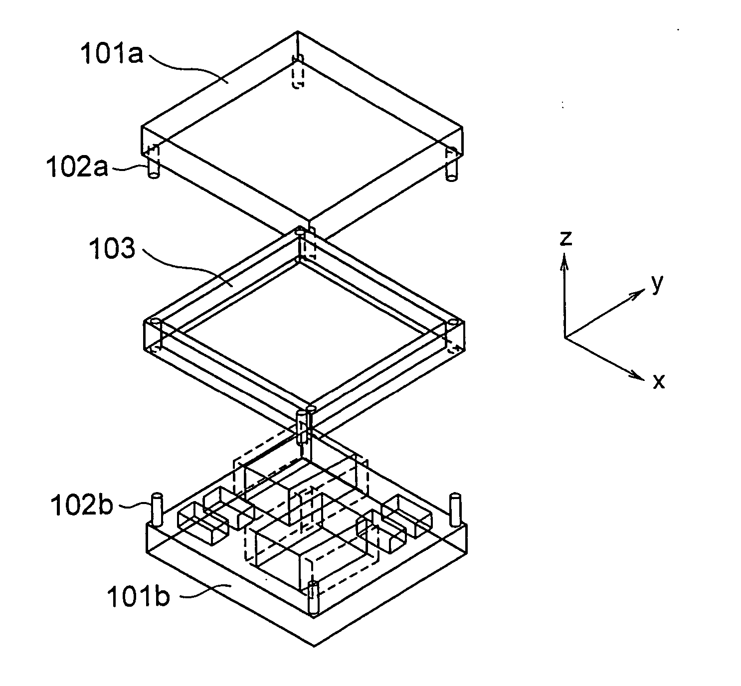
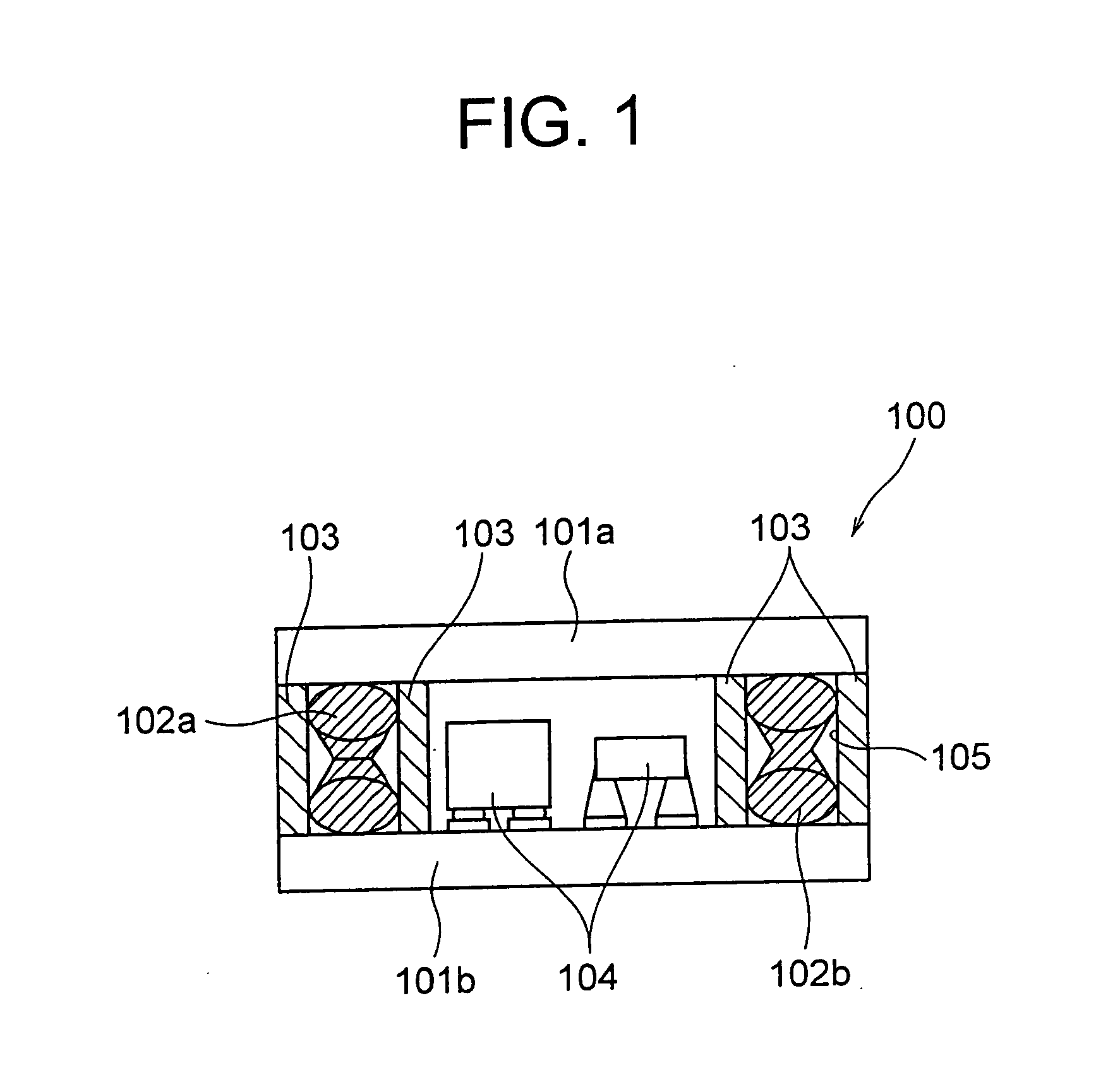
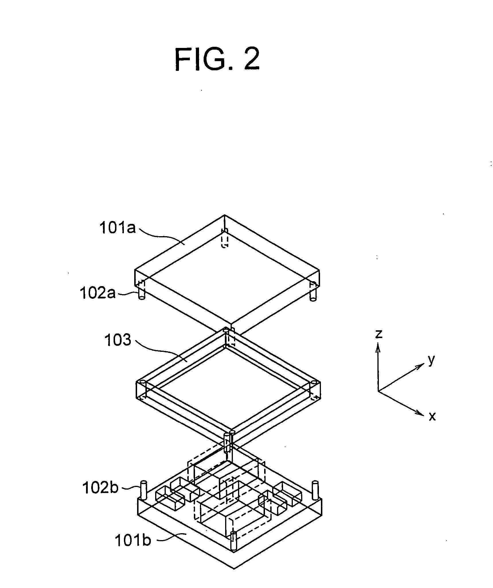
[0047] A stacked mounting structure 100 according to a first embodiment of the present invention will be described below. FIG. 1 shows a cross-sectional view of the stacked mounting structure 100. FIG. 2 shows a perspective view of the disassembled stacked mounting structure 100.

[0048] In FIG. 1, each of a first substrate 101a and a second substrate 101b is in a flat plate form. A substrate such as an organic substrate, a ceramic substrate, a glass substrate, a Si substrate, a metal substrate, and a flexible substrate can be used for these two substrates 101a and 101b. Moreover, it is also possible to use a composite material substrate in which these substrates are combined. The first substrate 101a corresponds to a first member. The second substrate 101b corresponds to a second member.

[0049] A term substrate is used for the sake of convenience. However, without restricting to the substrate, the present invention is similarly applicable to any member which forms a mounting structu...

second embodiment

[0078] Next, a stacked mounting structure 200 according to a second embodiment will be described below. FIG. 3 shows a cross-sectional view of a state before joining the stacked mounting structure 200. Same reference numerals are assigned to components which are same as in the first embodiment, and repeated description is omitted.

[0079] In the second embodiment, as shown in FIG. 3, a height of the first protruding electrode 102a is Ha and a height of the second protruding electrode 102b is Hb, and a combined height Ha+Hb which is a total of the two heights Ha and Hb is more than a height Hc of the intermediate substrate 103. At the same time, each of the first protruding electrode 102a and the second protruding electrode 102b has a shape in which a front end is the narrowest.

[0080] In other words, the heights Ha and Hb of the first protruding electrode 102a and the second protruding electrode 102b respectively, and the height Hc (thickness) of the intermediate electrode 103 satisf...

third embodiment

[0086] Next, a stacked mounting structure 300 according to a third embodiment of the present invention will be described below. FIG. 4 shows a cross-sectional view of a state before joining the stacked mounting structure 300. Same reference numerals are assigned to components which are same as in the first embodiment, and the repeated description is omitted.

[0087] In the third embodiment, as shown in FIG. 4, in a state before joining each member, a maximum diameter Wa of the first protruding electrode 102a and the second protruding electrode 102b is smaller than a diameter Wc of the opening 105 in the intermediate substrate 105.

[0088] In other words, the maximum diameter Wa of the first protruding electrode 102a and the second protruding electrode 102b, and the diameter Wc of the opening in the intermediate substrate 103 satisfy the following equation (2).

Wc>Wa  (2)

[0089] Next, an action of the third embodiment will be described below. By satisfying the equation (2), it is possibl...


PUM


Abstract

A stacked mounting structure includes at least two substrates namely a first substrate on which a first protruding electrode is formed and a second substrate on which a second protruding electrode is formed, and an intermediate substrate which is disposed between the first substrate and the second substrate, and which connects the first substrate and the second substrate by leaving a predetermined gap between the first substrate and the second substrate. Mounted components are disposed in the gap between the first substrate and the second substrate. The first protruding electrode and the second protruding electrode are connected in an opening which is provided in the intermediate substrate.

Description

CROSS-REFERENCE TO RELATED APPLICATION [0001] The present application is based upon and claims the benefit of priority from the prior Japanese Patent Application No. 2005-370157 filed on Dec. 22, 2005; the entire contents of which are incorporated herein by reference. BACKGROUND OF THE INVENTION [0002] 1. Field of the Invention [0003] The present invention relates to a stacked mounting structure, and particularly to a three-dimensional stacked mounting structure which is made by stacking a plurality of members in a directions of thickness of the members. [0004] 2. Description of the Related Art [0005] For a structure which includes substrates on which electronic components are mounted, various structures have been hitherto proposed (refer to Japanese Patent Application Kokoku (Post Exam Application) No. Hei 4-38417 and Japanese Patent Application Laid-open Publication No. Hei 11-111914 for example). In Japanese Patent Application Kokoku (Post Exam Application) No. Hei 4-38417, a mou...

Claims


Application Information

Patent Timeline
Patent Type & Authority Applications(United States)
IPC IPC(8): H01L23/52
CPCB81B2207/012B81B2207/017B81C1/00301B81C1/00333H01L21/50H01L2224/16H05K2201/0367H05K2201/0379H05K2201/042H05K2201/2018H05K1/144
Inventor SEKIDO, TAKANORIKONDOH, YOU
Owner OLYMPUS CORP
Why Eureka
Try Eureka