Optical Element Molding Device

a molding device and optical element technology, applied in the field of optical element molding devices, can solve the problems of affecting the structure easily induces deviations on the optically functional surfaces, and the lower mold elements greatly affect the aberration of the molded optical elements, and achieves excellent maintenance properties

Inactive Publication Date: 2007-07-19
FUJI PHOTO OPTICAL CO LTD
View PDF1 Cites 42 Cited by
  • Summary
  • Abstract
  • Description
  • Claims
  • Application Information

AI Technical Summary

Benefits of technology

[0009]The present invention relates to an optical element molding device that enables molding optical elements by constraining the deviation and inclination of the axes in upper and lower mold elements according to a simple structure that works excellently and that has excellent maintenance properties.

Problems solved by technology

However, because of molding errors on the optically functional surfaces of the optical elements, a beam irradiated from one point does not completely converge after transmission through the optical elements, and deviations resulting in aberrations occur.
In these molding devices, a minimum clearance is required between the upper and lower mold elements and the cavity mold element or elements, so the structures easily induce deviations on the optically functional surfaces molded by the upper and lower mold elements.
In particular, the axial inclination of the upper and lower mold elements greatly affects the aberrations of the molded optical elements.
In other words, even for the processing accuracy of the contact surface with the upper and lower heating plates in the second cavity mold element, if the processing accuracy of the contact surface with the second cavity mold element in the upper and lower heating plates cannot be sufficiently obtained, aberrations of the molded lens will be induced by the axial inclination of the upper and lower mold elements.
Therefore, even though processing of the contact surfaces of the upper and lower heating plates with the second cavity mold element is required with high accuracy, because the device itself with the upper and lower heating plates has a large configuration, it is difficult to process the device itself with high accuracy.
Moreover, even if the contact surfaces are processed with high accuracy, maintenance is required because the surface accuracy of the contact surfaces decreases due to abrasion or damage during the repetition of the lens molding process.
However, when maintaining the upper and lower heating plates, it is necessary to disassemble them from the molding device so that reprocessing the surfaces and reassembling the elements leads to the maintenance process itself becoming complex.

Method used


Image

  • Optical Element Molding Device
  • Optical Element Molding Device
  • Optical Element Molding Device

Examples


embodiment 1

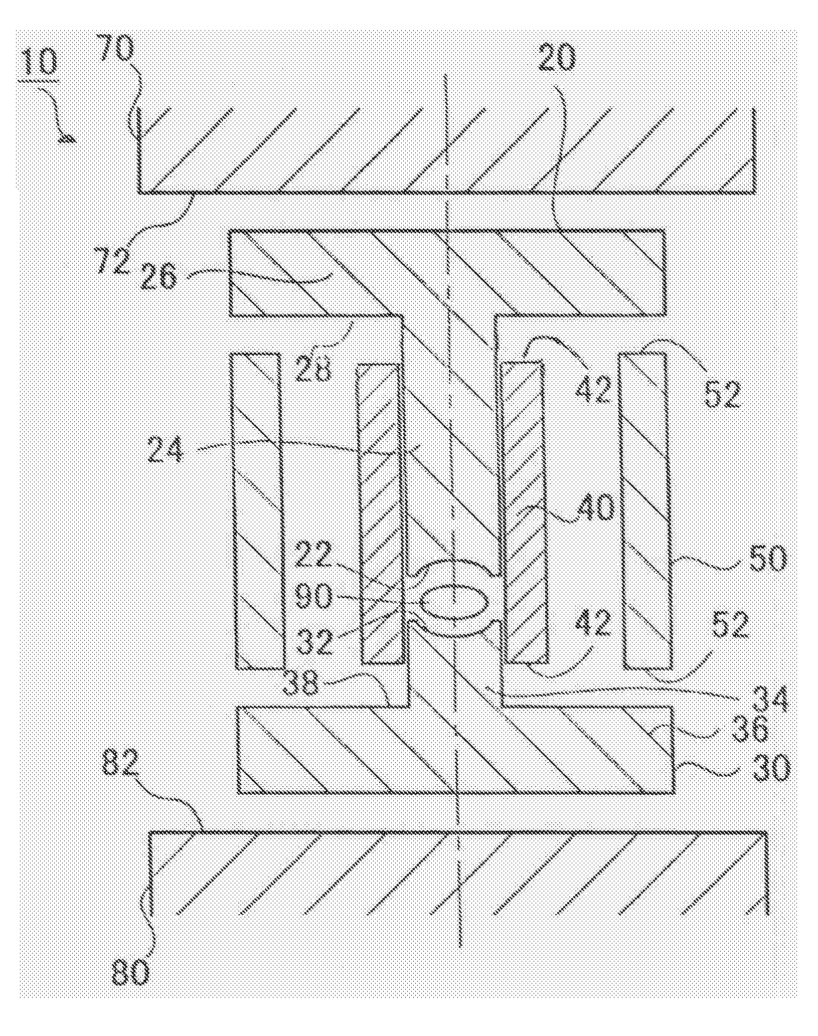
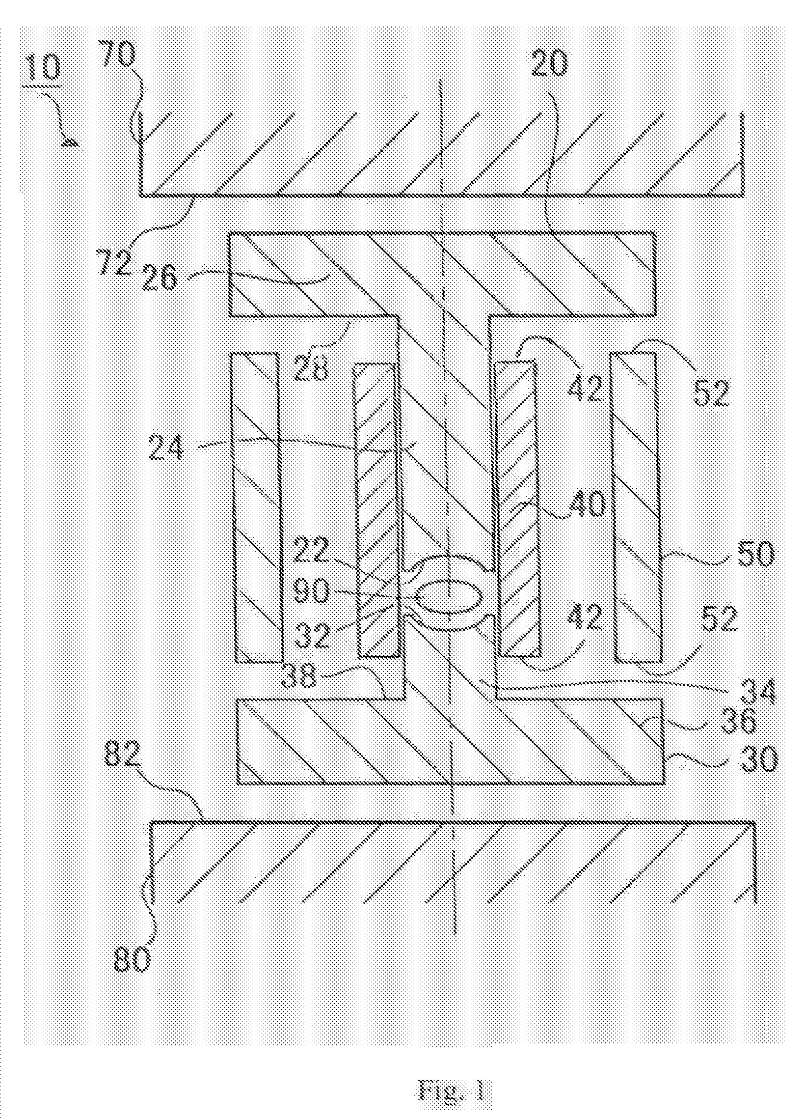
[0021]FIG. 1 shows an exploded cross-sectional view of the optical element molding device of Embodiment 1 of the present invention. The molding device 10 shown in FIG. 1 includes a pair of upper and lower mold elements 20 and 30, a first cavity mold element 40, a second cavity mold element 50, and a pair of upper and lower pressuring plates 70 and 80. Hereinafter, characteristics of each component contained in the related optical element molding device 10 are described.

[0022]Each of the upper mold element 20 and the lower mold element 30 includes a pedestal, 26 and 36, respectively, and a shaft, 24 and 34, respectively, projecting from each pedestal. The pedestals 26 and 36 each have a transverse section that is larger than those of the shafts 24 and 34, respectively. The upper and lower mold elements 20 and 30 have outer surfaces on the shafts 24 and 34 that are inside the first cavity mold element 40 and adjacent the inner surface of the first cavity mold element 40. Flanges 28 an...

embodiment 2

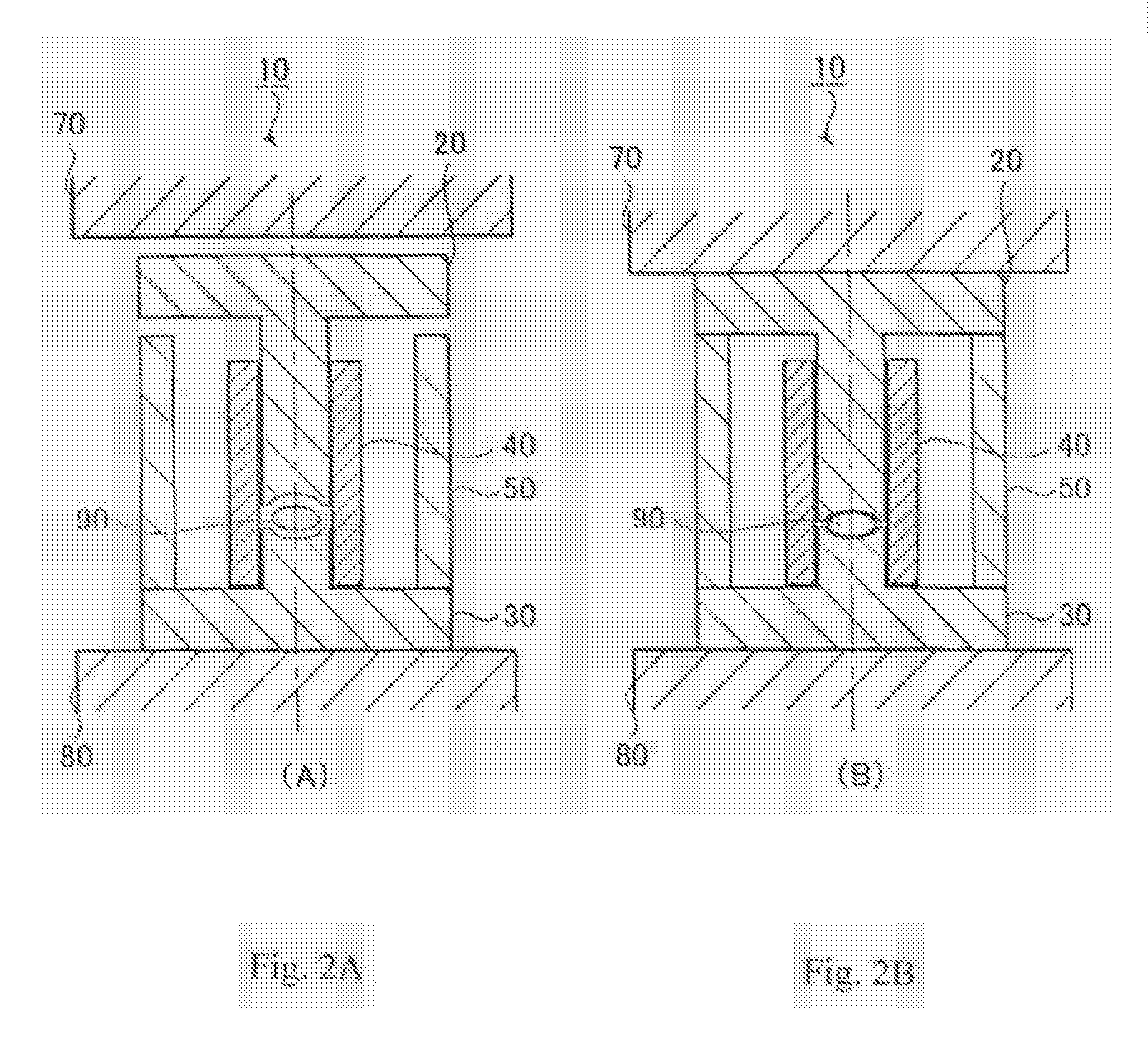
[0036]Next an optical element molding device related to a second embodiment, Embodiment 2, of the present invention is described. FIG. 3 shows a cross-sectional view of the optical element molding device of Embodiment 2 of the present invention. Embodiment 2 is similar to Embodiment 1, and therefore much of its operation may be understood from the previous discussion of Embodiment 1 and FIGS. 1, 2A, and 2B. In Embodiment 2, the same reference symbols as in Embodiment 1 are used for components that may be the same as in Embodiment 1, and components that are different but correspond to components of Embodiment 1 are referenced by the same reference symbol with a prime symbol added, as shown in FIG. 3. The optical element molding device 10′ of Embodiment 2 is different from Embodiment 1 in that the second cavity mold element 50′ comes into contact with only one of the upper mold element 20′ or the lower mold element 30. FIG. 3 illustrates the situation of the second cavity mold element...

embodiment 3

[0044]Next, an optical element molding device related to a third embodiment, Embodiment 3, of the present invention is described. FIG. 5 shows a cross-sectional view of the optical element molding device of Embodiment 3 of the present invention. Embodiment 3 is similar to Embodiment 1, and therefore much of its operation may be understood from the previous discussion of Embodiment 1 and FIGS. 1, 2A, and 2B. In Embodiment 3, the same reference symbols as in Embodiment 1 are used for components that may be the same as in Embodiment 1 and components that are different but correspond to components of Embodiment 1 are referenced by the same reference symbol with a prime symbol added, unless the components have been previously referenced with a prime symbol with regard to Embodiment 2, in which case the same reference symbol with two prime symbols added are used for Embodiment 3. As shown in FIG. 5, the optical element molding device 10″ of Embodiment 3 is different from Embodiments 1 and...


PUM

PropertyMeasurementUnit
optical functionaaaaaaaaaa
weightaaaaaaaaaa
densityaaaaaaaaaa

Abstract

An optical element molding device includes upper and lower mold elements and first and second cavity mold elements. Each of the upper and lower mold elements includes a pedestal and a shaft projecting along a common axis from a flange surface of each pedestal. An optical function transferring surface is formed at the tip of each shaft with the tips facing one another along the common axis. The first cavity mold element extends around these tips and the common axis for molding an optical element by heating and pressuring an optical material arranged between the upper and lower mold elements by their relative movement toward one another along the common axis guided by the first cavity mold element. Various surfaces contact one another in order to limit relative movement of the upper and lower mold elements along the common axis during molding and constrain axial inclination of these mold elements.

Description

FIELD OF THE INVENTION[0001]The present invention relates to an optical element molding device and particularly relates to an optical element molding device that enables molding an optical element with high accuracy.BACKGROUND OF THE INVENTION[0002]Associated with recent steps toward miniaturization, light weight, and providing multiple functions in optical apparatuses, various optical elements for use in optical systems have been developed. In particular, in products that use a lens with an optical disc, including pickup lenses used in optical instruments, such as DVDs (digital versatile disks), higher accuracy and higher numerical apertures of the optical elements are in demand. In addition, in Blu-ray Discs (large capacity phase change discs), in order to realize high density data memories, lenses with high numerical apertures are used along with a blue violet laser having a short wavelength, and it is anticipated that the demand for optical elements with higher numerical apertur...

Claims


Application Information

Patent Timeline
Patent Type & Authority Applications(United States)
IPC IPC(8): B29C43/00B29C43/52B29C35/02
CPCB29C43/021B29C43/361B29C2043/3618B29C2043/5858C03B2215/72B29D11/005B29L2011/0016C03B11/08C03B2215/60B29D11/00009
Inventor UTSUGI, MASANORI
Owner FUJI PHOTO OPTICAL CO LTD
Why Eureka
Try Eureka