Liquid crystal display device, driving method thereof, liquid crystal television having the liquid crystal display device and liquid crystal monitor having the liquid crystal display device

a technology of liquid crystal display device and driving method, which is applied in the direction of instruments, static indicating devices, etc., can solve the problems of flicker, display quality of moving image, inferior display property of moving image in hold mode, etc., and achieve the effect of lessening or decreasing

Active Publication Date: 2007-07-26
SHARP KK
View PDF19 Cites 37 Cited by
  • Summary
  • Abstract
  • Description
  • Claims
  • Application Information

AI Technical Summary

Benefits of technology

[0032] At least one embodiment of the present invention was made with at least one of the foregoing problems in mind. An object of at least one embodiment of the present invention is to provide (i)a liquid crystal display device which may, for example, lessen or even avoid voltage drop caused by a gat

Problems solved by technology

The deviation between the visual line and the display condition results in a blur image, so that a moving image display property in the hold mode is inferior to that in the impulse mode.
Recently, the TFT liquid crystal panel has been being widely used in TV or the like, and has raised problems such as display quality of a moving image and a viewing angle property of the liquid crystal panel as described above.
When the correction is not performed, the luminance varies between polarities, so that flicker occurs.
Howeve

Method used


Image

  • Liquid crystal display device, driving method thereof, liquid crystal television having the liquid crystal display device and liquid crystal monitor having the liquid crystal display device
  • Liquid crystal display device, driving method thereof, liquid crystal television having the liquid crystal display device and liquid crystal monitor having the liquid crystal display device
  • Liquid crystal display device, driving method thereof, liquid crystal television having the liquid crystal display device and liquid crystal monitor having the liquid crystal display device

Examples


embodiment 1

[0096] One embodiment of the present invention is described below with reference to FIGS. 1 to 5 and FIGS. 8 to 12.

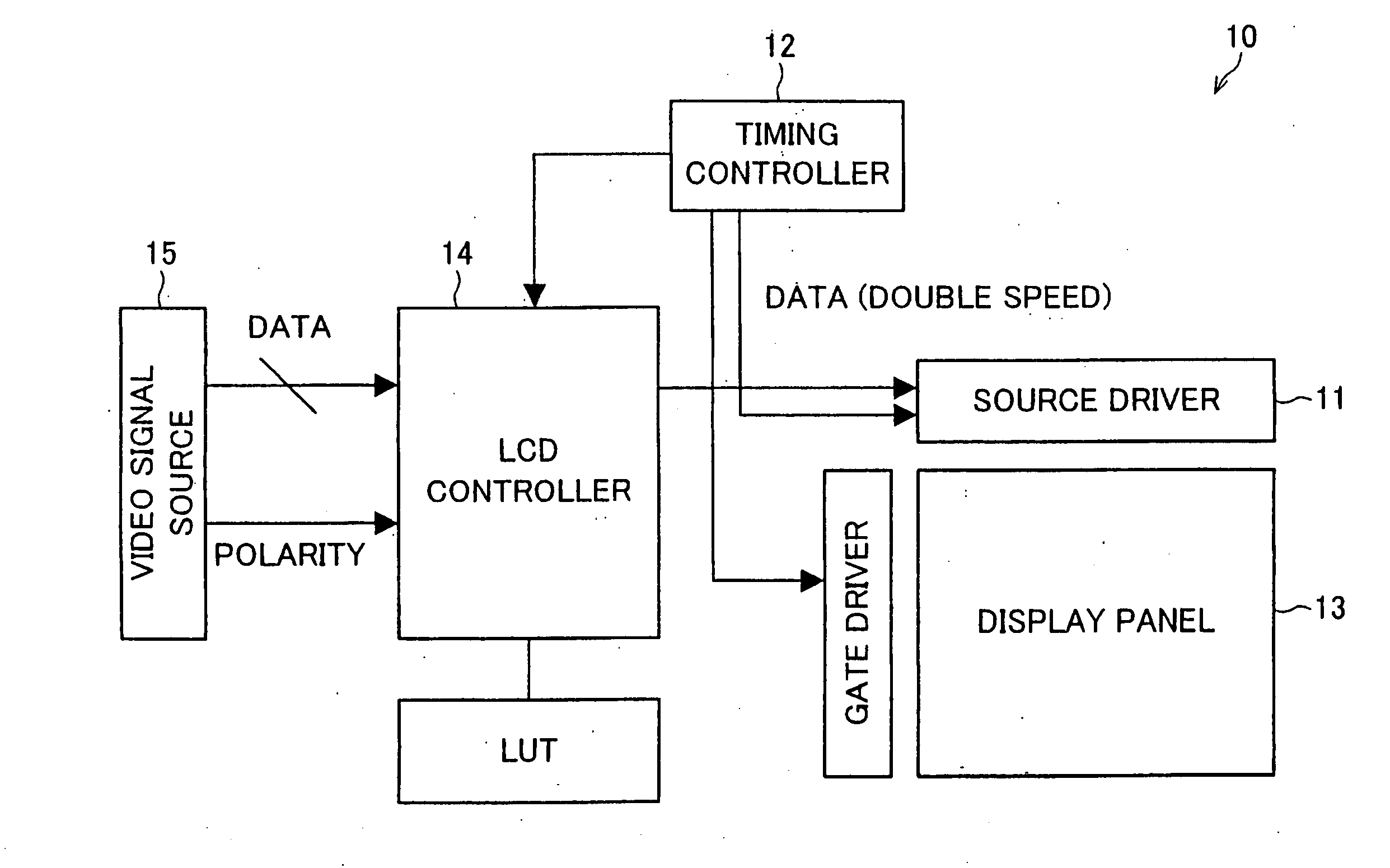
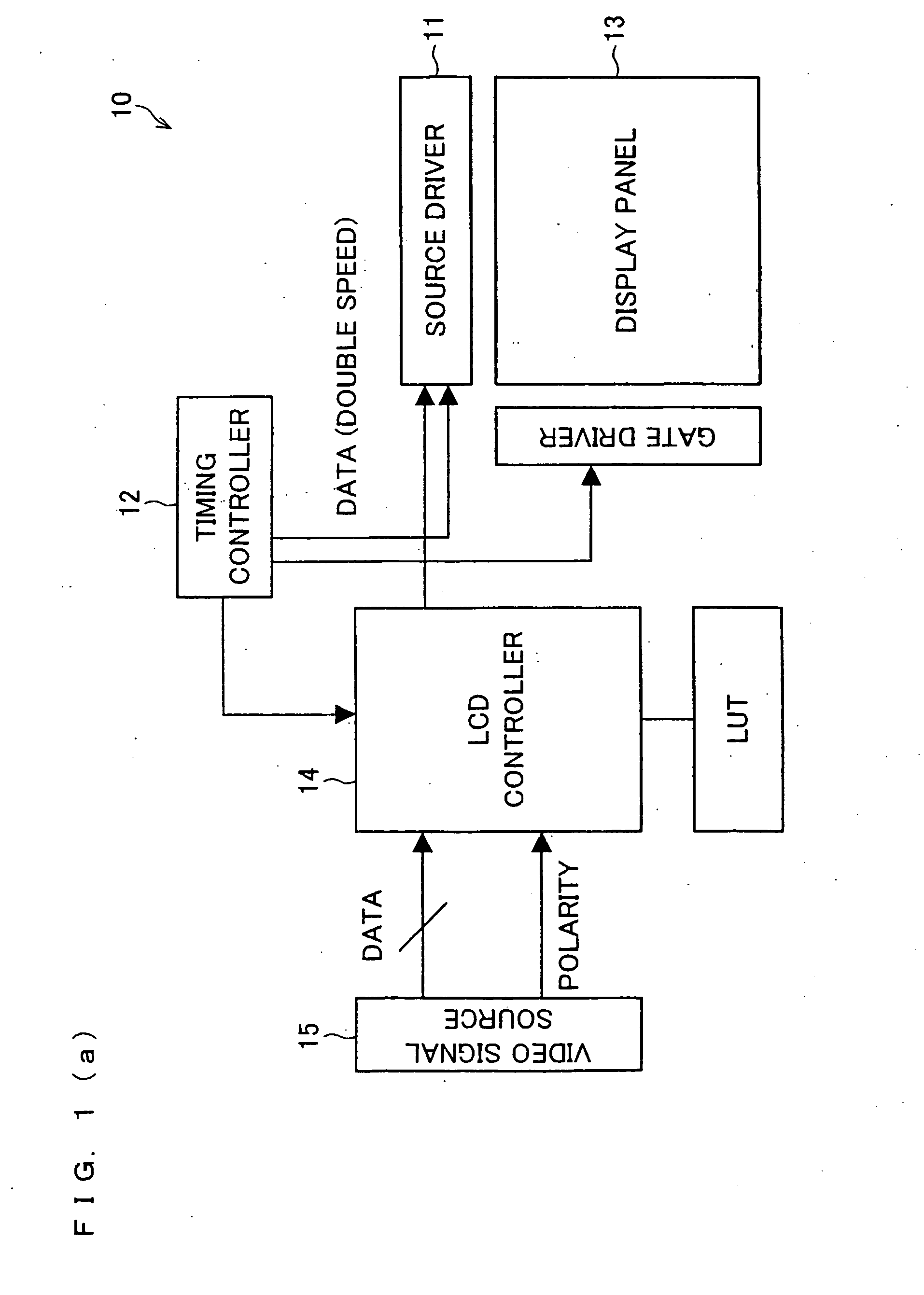
[0097] As shown in FIG. 8, a display panel 13 of a liquid crystal display device 10 of an example embodiment has a sandwich structure in which a liquid crystal layer 3 is provided between a TFT (thin film transistor) glass substrate 1 and a counter glass substrate 2. A counter electrode 4 is provided on an entire surface of the counter glass substrate 2, and a TFT element 6 is provided on each pixel 5 in the TFT glass substrate 1 as shown in FIGS. 9(a) and 9(b), and a drain of the TFT element 6 is connected to a pixel electrode 7.

[0098] On the TFT glass substrate 1, source lines 8 serving as data signal lines each of which supplies a data voltage to the TFT element 6 are vertically provided, and gate lines 9 serving as scanning signal lines each of which turns ON the TFT element 6 are horizontally provided. Each of the source lines 8 is connected to a source of the TF...

embodiment 2

[0189] Another embodiment of the present invention is described below with reference to FIGS. 6 to 7. Note that, an example embodiment is arranged in the same manner as Embodiment 1 except for an arrangement described below. Further, for convenience in description, the same reference numbers are given to members having the same functions as members of Embodiment 1, and description thereof is omitted.

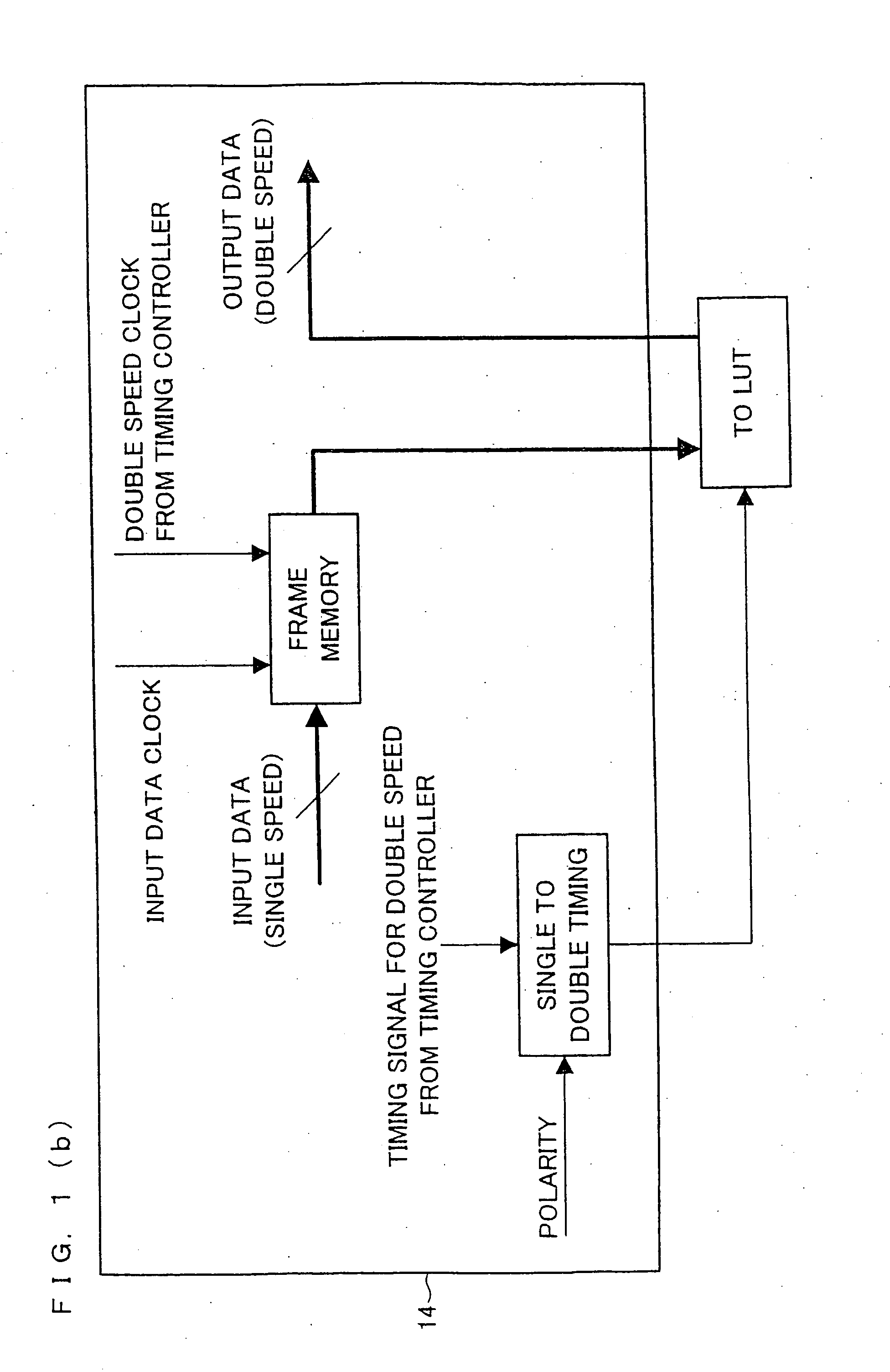
[0190] In order to lessen or even avoid the influence of the voltage drop which is caused by the gate-drain capacitance of the thin film transistor in case of adopting the time-division driving, a source driver input gradation value is converted in each polarity in Embodiment 1. However, embodiments of the present invention are not limited to such solution. It is possible to improve on or even solve the foregoing problem by arranging the liquid crystal display device so that: for example, the driver is designed so that the source driver input signal is inputted in the former and latter ...

embodiment 3

[0205] Another embodiment of the present invention is described below with reference to FIGS. 18 to 23. Note that, an example embodiment is arranged in the same manner as Embodiment 1 except for an arrangement described below. Further, for convenience in description, the same reference numbers are given to members having the same functions as members of Embodiment 1, and description thereof is omitted.

[0206] In Embodiment 2, the reference voltage generation circuit 16 prepares plural combinations of output voltages respectively corresponding to positive and negative polarities in the former sub-frame and positive and negative polarities in the latter sub-frame in an entire range from 0 gradation 0 to 255 gradations.

[0207] Meanwhile, an example embodiment describes a reference voltage generation circuit in which a large number of black (minimum or relative minimum luminance) voltages and a large number of white (maximum or relative maximum luminance) voltages are outputted. FIG. 18...


PUM


Abstract

A device is provided for setting a voltage applied to each of data signal lines so as to correct a voltage, applied to the pixel, which corresponds to a gradation data signal in each of sub-frames of a single frame. As such, voltage drop, caused by a combination of voltages of the gradation data signal in each of the sub-frames, may be partially or even fully compensated. On this account, it is possible to provide a liquid crystal display device which can lessen or even avoid an influence of the voltage drop caused by, for example, gate-drain capacitance of the thin film transistor in case of adopting time-division driving, and/or a method for driving the liquid crystal display device.

Description

TECHNICAL FIELD [0001] The present invention generally relates to (i) a liquid crystal display device, (ii) a driving method of the liquid crystal display device, (iii) a liquid crystal television having the liquid crystal display device, and / or (iv) a liquid crystal monitor having the liquid crystal display device. BACKGROUND ART [0002] [Explanation of a TFT (thin film transistor) liquid crystal panel][0003] A TFT liquid crystal panel uses a nonluminous element. Generally, a backlight or a reflection plate is provided on a back side of the TFT liquid crystal panel, and the TFT liquid crystal panel applies a voltage to liquid crystal on the basis of luminance of the back light or the like so as to change a transmittance of the liquid crystal, thereby displaying an image. When a voltage corresponding to display gradation data is applied to a pixel of the TFT liquid crystal panel, a transmittance (liquid crystal alignment) of the pixel is maintained until a next voltage is applied, an...

Claims


Application Information

Patent Timeline
IPC IPC(8): G09G3/36G02F1/133G09G3/20
CPCG09G3/2025G09G3/3614G09G3/3648G09G2320/028G09G2320/0219G09G2320/0247G09G2320/0261G09G2310/061
Inventor MIYATA, HIDEKAZU
Owner SHARP KK
Why Eureka
Try Eureka