Semiconductor device

a semiconductor and device technology, applied in semiconductor devices, instruments, electrical equipment, etc., can solve the problems of minute semiconductor elements manufactured on a substrate degrading or being destroyed, degradation or destruction of semiconductor elements connected to pixel electrodes, etc., to relieve sudden changes, and prevent electrostatic discharge damage

Inactive Publication Date: 2007-08-02
SEMICON ENERGY LAB CO LTD
View PDF48 Cites 44 Cited by
  • Summary
  • Abstract
  • Description
  • Claims
  • Application Information

AI Technical Summary

Benefits of technology

[0013] If the protecting means is a transistor of which the drain electrode and the gate electrode are connected, a source electrode of the transistor is connected to an electric power source line. The transistor discharges the electric charge that builds up in the pixel electrode to the electric power source line, and the electric potential of the pixel electrode is thus set to the same electric potential as that of the electric power source line, or to an electric potential conforming thereto. Sudden changes in the electric potential of the source electrode or the drain electrode of the transistor caused by the electric charge that builds up in the pixel electrode can thus be relieved.
[0014] If the protecting means is a diode, one electrode of the diode is connected to the pixel electrode, and the other electrode is connected to the electric power source line. The electric potential of the pixel electrode is set to the same electric potential as that of the electric power source line by discharging the electric charge that builds up in the pixel electrode to the electric power source line. Sudden changes in the electric potential of the source electrode or the drain electrode of the transistor caused by the electric charge that builds up in the pixel electrode can thus be relieved.
[0015] With the structure described above, the present invention relieves sudden changes in the electric potential of the source electrode or the drain electrode of the transistor due to electric charge that builds up in the pixel electrode, and prevents electrostatic discharge damage. Further, the present invention prevents electrostatic discharge damage during manufacturing processes, and in particular, electrostatic discharge damage in a state up through the manufacture of the pixel electrode.

Problems solved by technology

If this phenomenon develops in a free node such as an input terminal of the semiconductor device, then minute semiconductor elements manufactured on a substrate will degrade or be destroyed.
Sudden discharge of electric charge that has built up in the pixel electrodes leads to degradation or destruction of the semiconductor elements connected to the pixel electrodes.

Method used


Image

  • Semiconductor device
  • Semiconductor device
  • Semiconductor device

Examples


embodiment mode 1

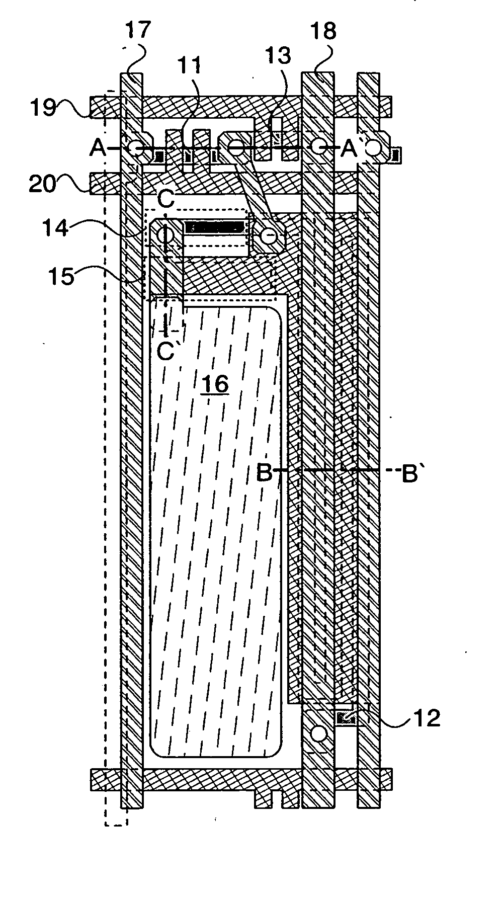
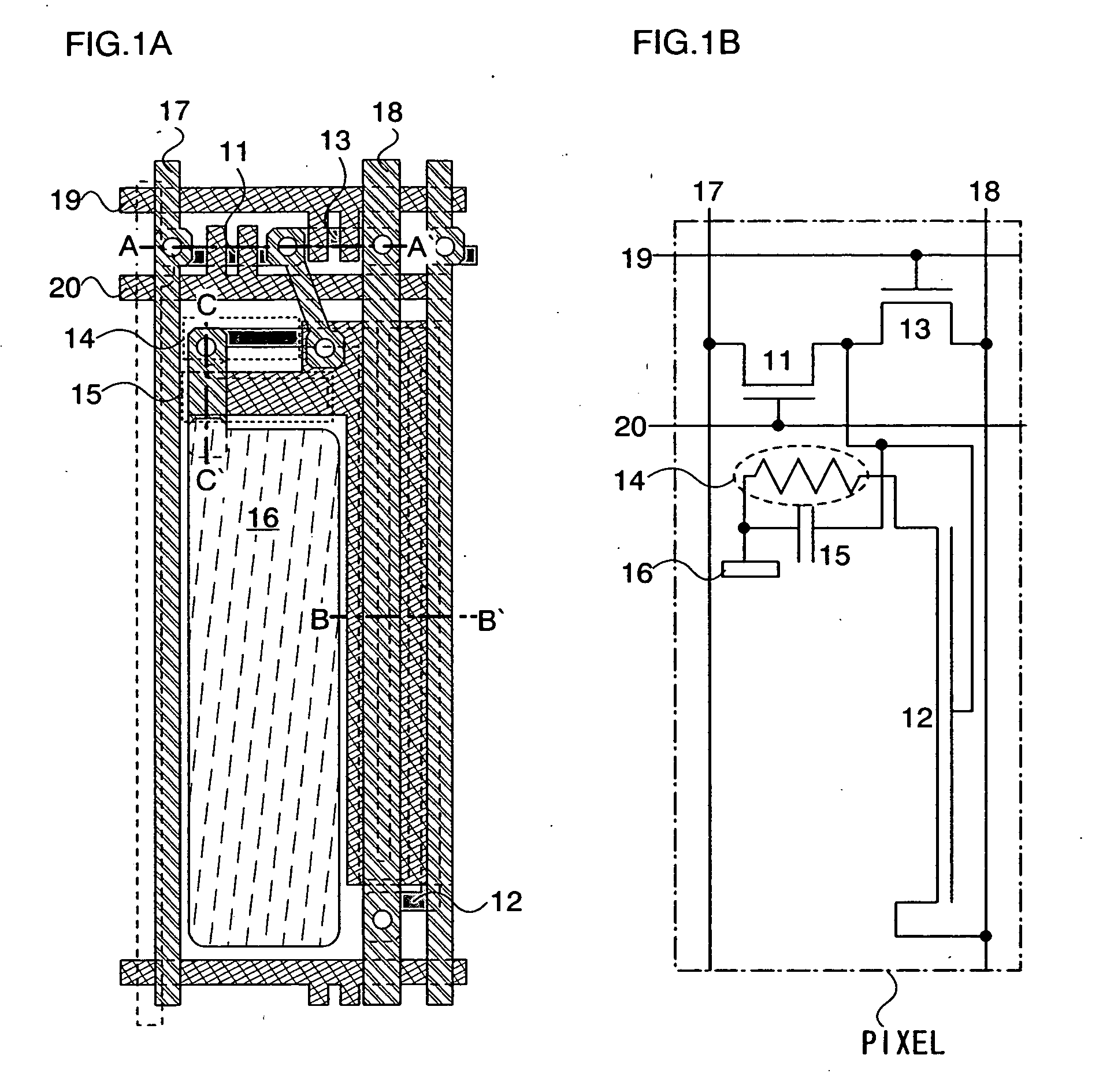
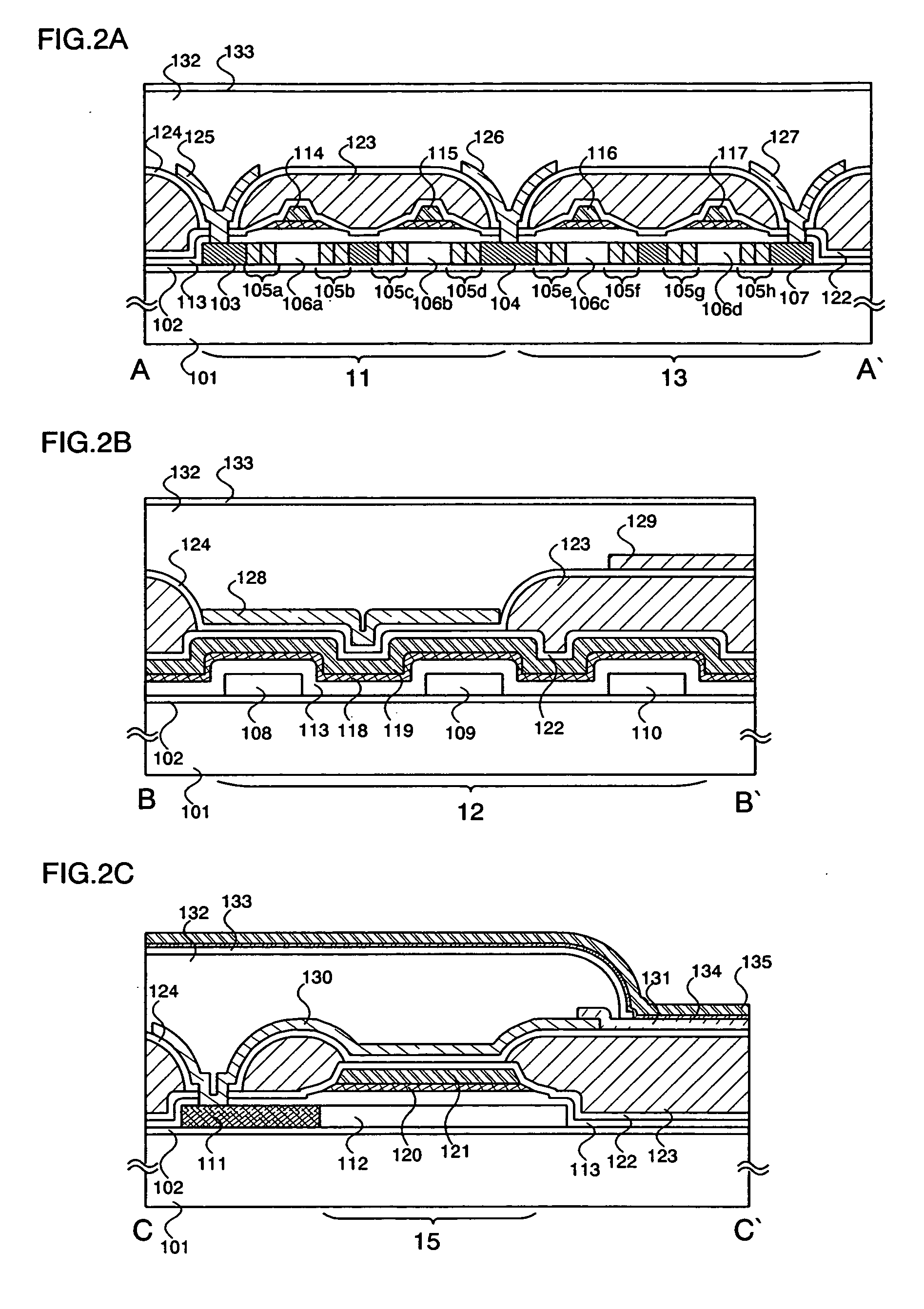
[0041] An embodiment mode of the present invention is explained using FIGS. 1A to 3. FIGS. 1A and 1B show a state up through the manufacture of a pixel electrode. FIG. 1A is a schematic diagram of a top view (masking diagram) of a pixel of a semiconductor device, and FIG. 1B is a circuit diagram that schematically expresses a circuit structure thereof. FIGS. 2A to 2C are cross sectional diagrams of the pixels of FIG. 1A. FIG. 3 is a photograph of a panel having an actually manufactured pixel, magnified to approximately 635 times with an optical microscope.

[0042] Each of the pixels shown in FIGS. 1A and 1B are disposed in a region surrounded by a signal line 17 and an electric power source line 18 arranged in a column direction, and a scanning line 20 and a reset line 19 arranged in a row direction. Further, each of the pixels has a switching transistor 11 (hereinafter written as the transistor 11), a driving transistor 12 (hereinafter written as the transistor 12), an erasing trans...

embodiment mode 2

[0065] An embodiment mode of the present invention is explained using FIGS. 4A to 9. FIGS. 4A to 6B show a state up through the manufacture of a pixel electrode. FIG. 4A to 6A are schematic diagrams of a top view (masking diagram) of a pixel of a semiconductor device, and FIG. 4B to 6B are circuit diagrams that schematically express a typical circuit structure thereof. FIGS. 7A to 7D are cross sectional diagrams of the pixels of FIGS. 4A to 6A. FIGS. 8 and 9 are photographs of a panel having an actually manufactured pixel, magnified to approximately 695 times with an optical microscope.

[0066] Each of the pixels shown in FIGS. 4A to 6B is disposed in a region surrounded by the signal line 17 and the electric power source line 18, which are arranged in a column direction, and the scanning line 20 and the reset line 19, which are arranged in a row direction. Further, each of the pixels has the transistors 11 to 13, and the pixel electrode 16. Each of the pixels shown in FIGS. 4A and 4...

embodiment mode 3

[0086] Circuit diagrams in a state up through the manufacture of the pixel electrode are shown in Embodiment Modes 1 and 2, discussed above, but a circuit diagram of a state up through the manufacture of a light-emitting element is explained in this embodiment mode by using FIGS. 10A to 10D.

[0087] Pixels shown in FIGS. 10A to 10D correspond to the pixels shown in FIGS. 1B, 4B, 5B, and 6B, respectively. A protecting means, which corresponds to one or a plurality of elements selected from the resistor element 14, the capacitor element 15, and the rectifying element 22, is formed between the transistor 12 and a pixel electrode of a light-emitting layer 25 in all of the pixels. Further, a counter electrode of the light-emitting element 25 is connected to the electric power source line 24.

[0088] In addition, although the transistors 11 and 13 are n-channel and the transistor 12 is p-channel in each of the pixels shown in FIGS. 10A to 10D, the present invention is not limited in particu...


PUM


Abstract

Semiconductor elements deteriorate or are destroyed due to electrostatic discharge damage. The present invention provides a semiconductor device in which a protecting means is formed in each pixel. The protecting means is provided with one or a plurality of elements selected from the group consisting of resistor elements, capacitor elements, and rectifying elements. Sudden changes in the electric potential of a source electrode or a drain electrode of a transistor due to electric charge that builds up in a pixel electrode is relieved by disposing the protecting means between the pixel electrode of the light-emitting element and the source electrode or the drain electrode of the transistor. Deterioration or destruction of the semiconductor element due to electrostatic discharge damage is thus prevented.

Description

BACKGROUND OF THE INVENTION [0001] 1. Field of the Invention [0002] The present invention resides in a technical field relating to semiconductor devices. In particular, the present invention resides in a technical field relating to semiconductor devices that use a semiconductor element such as a transistor. [0003] 2. Description of the Related Art [0004] Development of semiconductor devices having light-emitting elements has been advanced in recent years. In addition to the existing advantages of liquid crystal display devices, the semiconductor devices also have characteristics such as fast response speed, superior dynamic display, and a wide angle of view. The semiconductor devices are attracting attention as flat panel displays for the next generation of mobile devices, which will be capable of utilizing dynamic contents. [0005] A semiconductor device having light-emitting elements has a plurality of pixels, which each have a light-emitting element and at least two transistors. T...

Claims


Application Information

Patent Timeline
Patent Type & Authority Applications(United States)
IPC IPC(8): H01L29/04
CPCG09G3/3233G09G2310/0251H01L27/1214H01L27/0248H01L27/12G09G2330/04H01L27/1255H01L27/1222H01L29/78675H10K59/1213H10K59/123H10K59/131H10K59/1216
Inventor YAMAZAKI, SHUNPEIHAYAKAWA, MASAHIKOTANADA, YOSHIFUMIOSAME, MITSUAKIANZAI, AYAFUKUMOTO, RYOTA
Owner SEMICON ENERGY LAB CO LTD
Why Eureka
Try Eureka