Phased array systems and methods

a phased array and array technology, applied in the direction of antennas, electrical equipment, radio transmission, etc., can solve the problems of incompatibility with low temperature substrates, inability to meet the requirements of low temperature substrates, and relatively expensive processes

Active Publication Date: 2007-08-02
ONED MATERIAL INC
View PDF50 Cites 94 Cited by
  • Summary
  • Abstract
  • Description
  • Claims
  • Application Information

AI Technical Summary

Problems solved by technology

However, amorphous silicon and organic semiconductors have performance limitations.
Polysilicon has showed improved performance, but requires relatively expensive processes, such as laser induced annealing, and is incompatible with low temperature substrates, such as cheap glass and plastics.
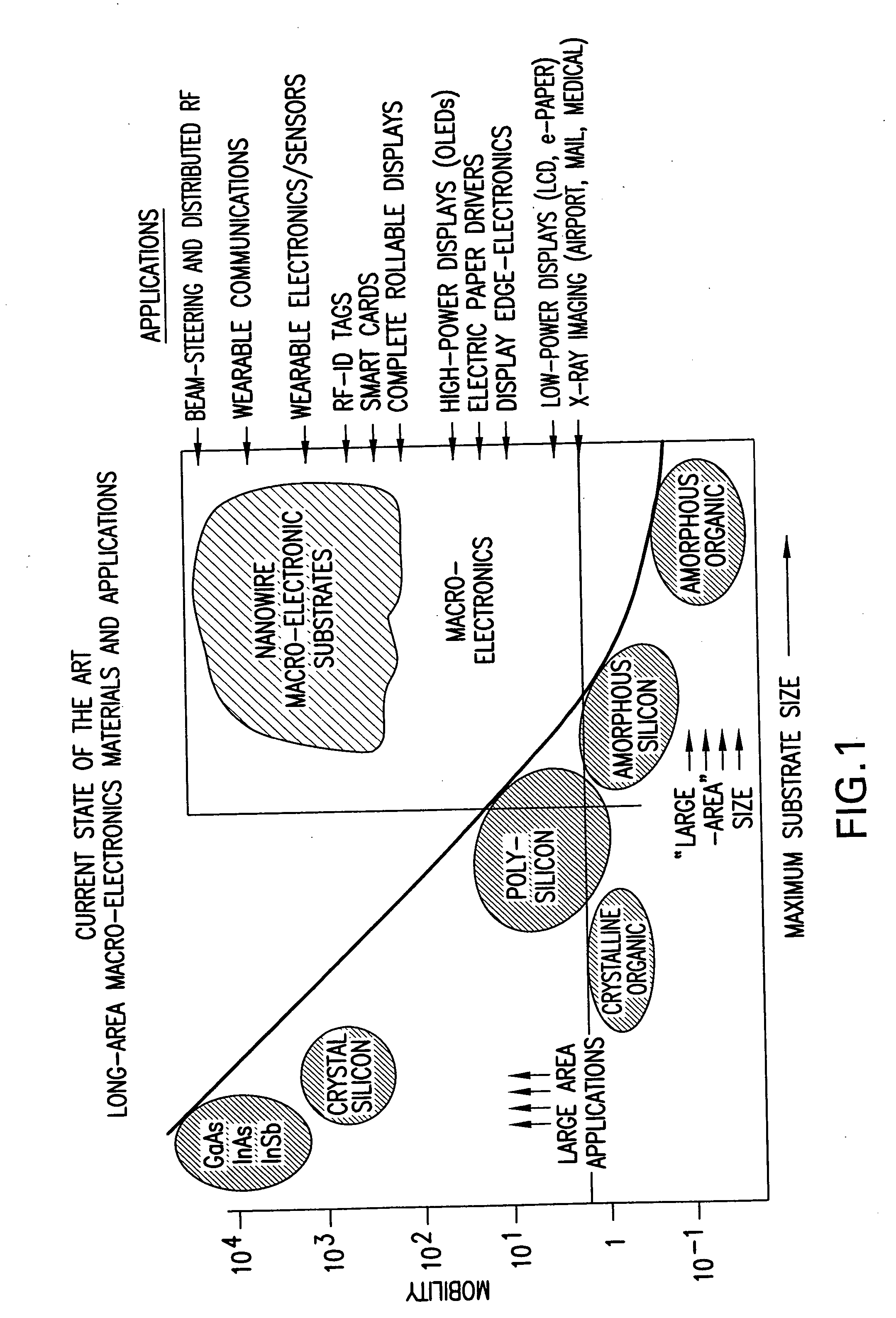
Traditional materials either have high performance but small substrate sizes (e.g., GaAs), or larger sizes with low performance (e.g., amorphous silicon or organics).
Current electronic materials can only access the most primitive large-area macroelectronics applications.
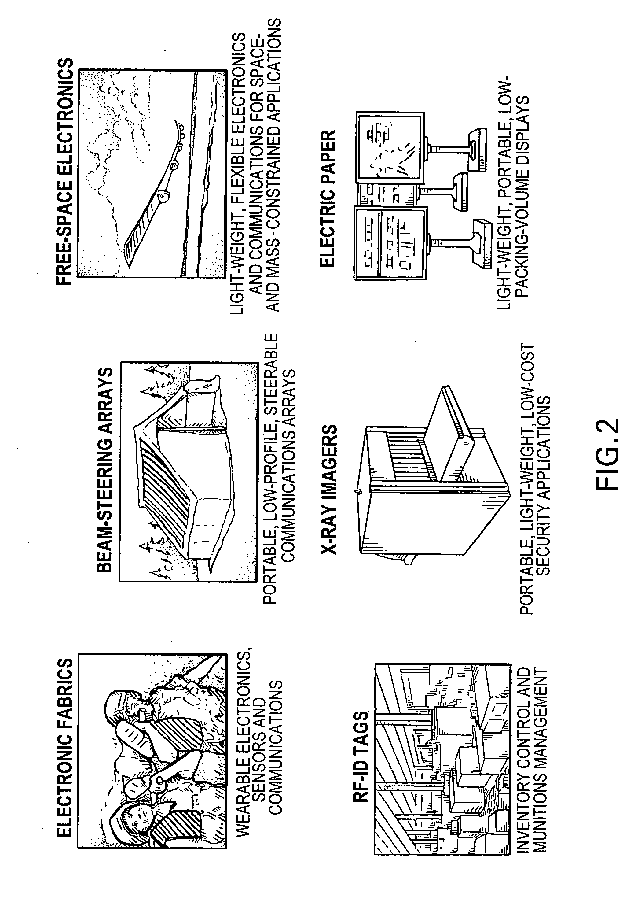
This leaves a tremendous void in materials characteristics, which has prevented the development of the highest-value macroelectronic applications, such as wearable communications and electronics, distributed sensor networks, and radio frequency (RF) beam-steering systems, to name a few.
InAs wafers, however, are currently limited to a maximum of 34 inches (8-10 cm) in diameter and are extremely brittle, making them inappropriate for use in such large-area distributed electronic circuits.
As such, the only methods currently available for fabricating such large-area circuits are to wire-bond or solder discrete transistors and components on the large-area active reflector, a costly and failure-prone alternative with inherent performance and efficiency limitations.
Today, even military applications of such arrays are limited to such examples as solid communications arrays on Navy destroyers; they cannot be implemented into mobile, let alone man-portable, communications systems.
A limiting factor in the area of RFID tag tracking systems is the cost of the tags.
Further limiting factors include the distance between the reader and tags, and the orientation of tag antennas relative to the reader antenna.
Current tag and reader technology is not capable of reading such a large number of items in a few seconds.
However, such technology is limited to relatively small size devices, such as headphones, and cannot be applied to the large objects mentioned above.

Method used


Image

  • Phased array systems and methods
  • Phased array systems and methods
  • Phased array systems and methods

Examples


Embodiment Construction

Introduction

[0104] In many ways, the electronics industry today is in the same position it was fifty years ago. At that time, the introduction of discrete transistors provided the world with unprecedented functionality. By integrating multiple discrete transistors together, functionality was further increased, leading to the broad availability of portable electronics. Unfortunately, at that time, integration was done by hand, causing the electronics industry to rapidly reach a plateau, beyond which integrating more than a few thousand individual transistors became prohibitive in terms of cost and yield. This phenomenon was referred to as the “Tyranny of Numbers”.

[0105] This practical limit, resulting from the need for heterogeneous integration of multiple discrete components, brought the integrated electronics industry to a standstill that was only resolved through the invention of a revolutionary new concept: the silicon microcircuit. The silicon microcircuit allowed seamless in...


PUM


Abstract

A phased array system having antennas, non-variable phase shifters, and switches. The non-variable phase shifters are configured to be coupled selectively to a transmitter or a receiver. A non-variable phase shifter is configured to shift a phase of an electromagnetic energy wave that traverses the non-variable phase shifter by a fraction of a period of the electromagnetic energy wave for a range of frequencies of the electromagnetic energy wave. At least one of the fraction and the range associated with the non-variable phase shifter is different from at least one of the fraction and the range associated with other non-variable phase shifters. The switches are configured to couple selectively the antennas to the non-variable phase shifters, the transmitter, or the receiver.

Description

CROSS-REFERENCE TO RELATED APPLICATIONS [0001] This application is a continuation-in-part of U.S. application Ser. No. 11 / 453,118, filed Jun. 14, 2006, which is a divisional of U.S. application Ser. No. 11 / 226,187, filed Sep. 14, 2005, now U.S. Pat. No. 7,083,104, which is a divisional of U.S. application Ser. No. 10 / 674,071, filed Sep. 30, 2003, now U.S. Pat. No. 7,051,945, each of which is incorporated herein in its entirety by reference. U.S. application Ser. No. 10 / 674,071 claims the benefit of U.S. Provisional Application No. 60 / 414,323, filed Sep. 30, 2002; 60 / 468,276, filed May 7, 2003; 60 / 474,065, filed May 29, 2003; and 60 / 493,005, filed Aug. 7, 2003, each of which is incorporated in U.S. application Ser. No. 10 / 674,071 in its entirety by reference. U.S. application Ser. No. 10 / 674,071 also claims the benefit of U.S. Provisional Application No. 60 / 445,421, filed Feb. 5, 2003, which is incorporated herein in its entirety by reference.BACKGROUND OF THE PRESENT INVENTION [0002...

Claims


Application Information

Patent Timeline
Patent Type & Authority Applications(United States)
IPC IPC(8): H01Q3/00H01Q3/12
CPCH01Q3/34
Inventor STUMBO, DAVID P.COMPTON, RICHARD
Owner ONED MATERIAL INC
Why Eureka
Try Eureka