Program method of flash memory capable of compensating read margin reduced due to charge loss

a technology of charge loss and program method, applied in the field of flash memory system, can solve the problems of increasing the time required for programming memory cells, difficult to know the state of the programmed memory cell, and difficulty in ensuring the read margin between states

Active Publication Date: 2007-08-09
SAMSUNG ELECTRONICS CO LTD
View PDF11 Cites 110 Cited by
  • Summary
  • Abstract
  • Description
  • Claims
  • Application Information

AI Technical Summary

Benefits of technology

[0011]An exemplary embodiment of the present invention provides a program method of a flash memory device including a plurality of memory cells for storing multi-bit data indicating one of a plurality of states. The program method may include programming selected memory cells with multi-bit data to correspond to one of a plurality of states. Programmed memory cells arranged within a predetermined threshold voltage region are detected. The predetermined region is selected by one of a first verify voltage, a read voltage and a second verify voltage. The second verify voltage being higher than the first verify voltage. The detected memory cells are programmed to have a threshold voltage equivalent to or higher than a second verify voltage corresponding to the respective states wherein the second verify voltages are set to have different voltage levels.

Problems solved by technology

Unfortunately, this leads to increase of time required for programming a memory cell to reach a desired state.
Accordingly, a threshold voltage increases due to an electric field coupling / F-poly coupling and a threshold voltage decreases due to HTS which makes it difficult to secure a read margin between states.
In particular, it is difficult to know a state of the programmed memory cell.
This problem becomes severe with the recent trend toward more complex semiconductor fabrication processes.

Method used


Image

  • Program method of flash memory capable of compensating read margin reduced due to charge loss
  • Program method of flash memory capable of compensating read margin reduced due to charge loss
  • Program method of flash memory capable of compensating read margin reduced due to charge loss

Examples


Embodiment Construction

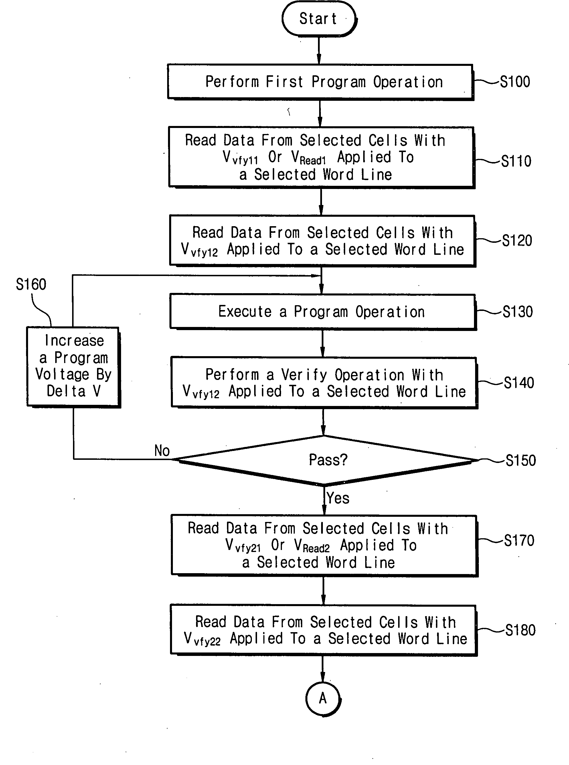
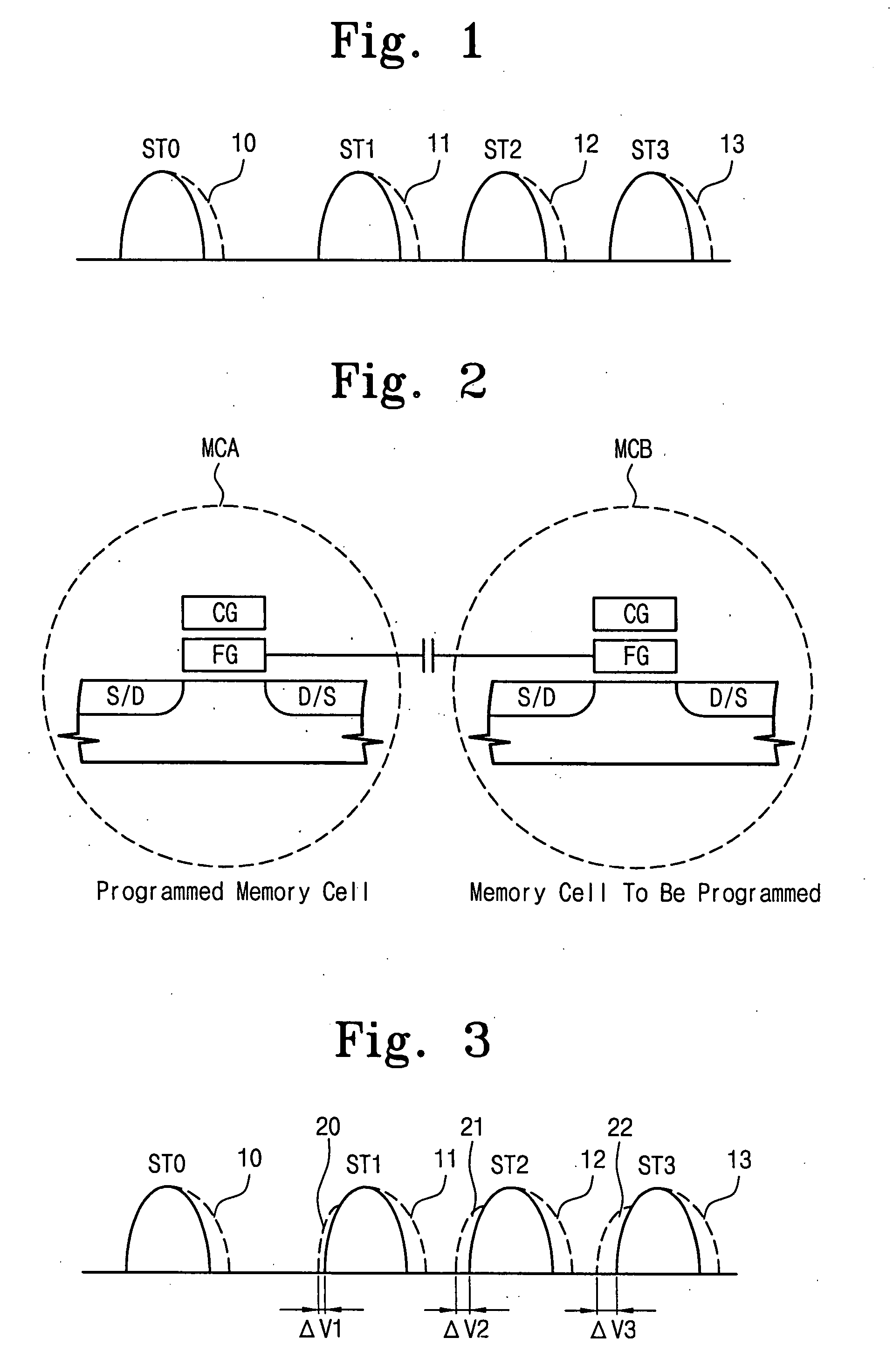
[0021]The present invention will now be described more fully hereinafter with reference to the accompanying drawings, in which preferred embodiments of the invention are shown. This invention, however, may be embodied in many different forms and should not be construed as limited to the embodiments set forth herein. Rather, these embodiments are provided so that this disclosure will be thorough and complete, and will fully convey the scope of the invention to those skilled in the art. In the drawings, like numbers refer to like elements throughout.

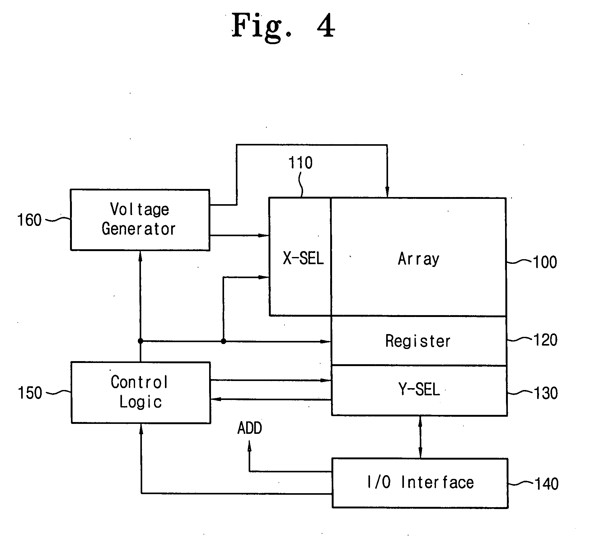
[0022]FIG. 4 is a block diagram of a flash memory device according to an embodiment of the present invention which comprises a memory cell array 100 for storing data information. The memory cell array 100 includes a plurality of memory blocks each having a memory cell configuration illustrated in FIG. 5.

[0023]FIG. 5 is a circuit diagram of a memory cell array illustrated in FIG. 4 comprising a memory block MB that includes a plurality of s...


PUM


Abstract

The present invention provides a program method of a flash memory device including a plurality of memory cells for storing multi-bit data indicating one of a plurality of states. The memory cells are subjected to a primary program operation. Those memory cells arranged within a specific region of respective states are subjected to a secondary program operation to have a threshold voltage equivalent to or higher than a verify voltage used in the primary program operation. Thus, although a threshold voltage distribution is widened due to an electric field coupling/F-poly coupling and HTS, a read margin between adjacent states may be sufficiently secured using the program method.

Description

BACKGROUND OF THE INVENTION[0001]1. Field of the Invention[0002]Embodiments of the invention relate to a flash memory system. More particularly, embodiments of the invention relate to a flash memory system capable of compensating for reduced read margins due to charge loss.[0003]This U. S non-provisional patent application claims priority under 35 U.S.C §119 of Korean Patent Application 2006-09781 filed on Feb. 1, 2006, the entirety of which is hereby incorporated by reference.[0004]2. Discussion of Related Art[0005]In recent years, storage devices such as volatile memory devices and non-volatile memory devices have been increasingly applied to MP3 players and mobile appliances such as, for example, portable multimedia players (PMPs), cellular phones, notebook computers, and personal digital assistances (PDAs). The MP3 players and the mobile appliances require mass storage devices for offering various functions (e.g., moving picture playback). Many efforts have been made for meeting...

Claims


Application Information

Patent Timeline
Patent Type & Authority Applications(United States)
IPC IPC(8): G11C11/34G11C16/04
CPCG11C11/5628G11C16/0483G11C16/12G11C2211/5621G11C16/3454G11C16/3459G11C16/3418G11C16/10G11C16/34
Inventor CHOI, KI-HWANLIM, YOUNG-HO
Owner SAMSUNG ELECTRONICS CO LTD
Why Eureka
Try Eureka