

Camera module
- Summary
- Abstract
- Description
- Claims
- Application Information
AI Technical Summary
Benefits of technology
Problems solved by technology
Method used
Image

Examples
first embodiment
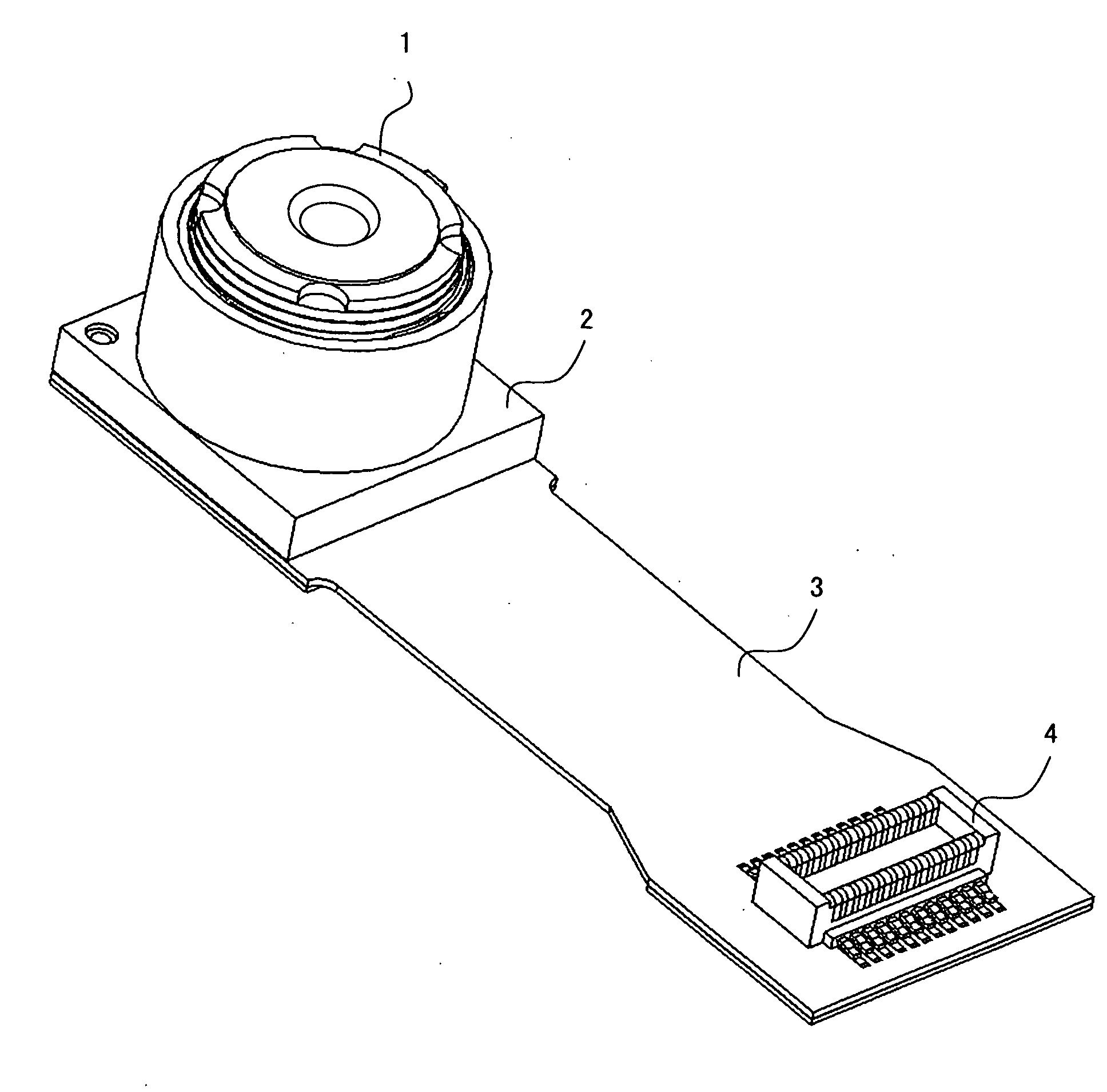
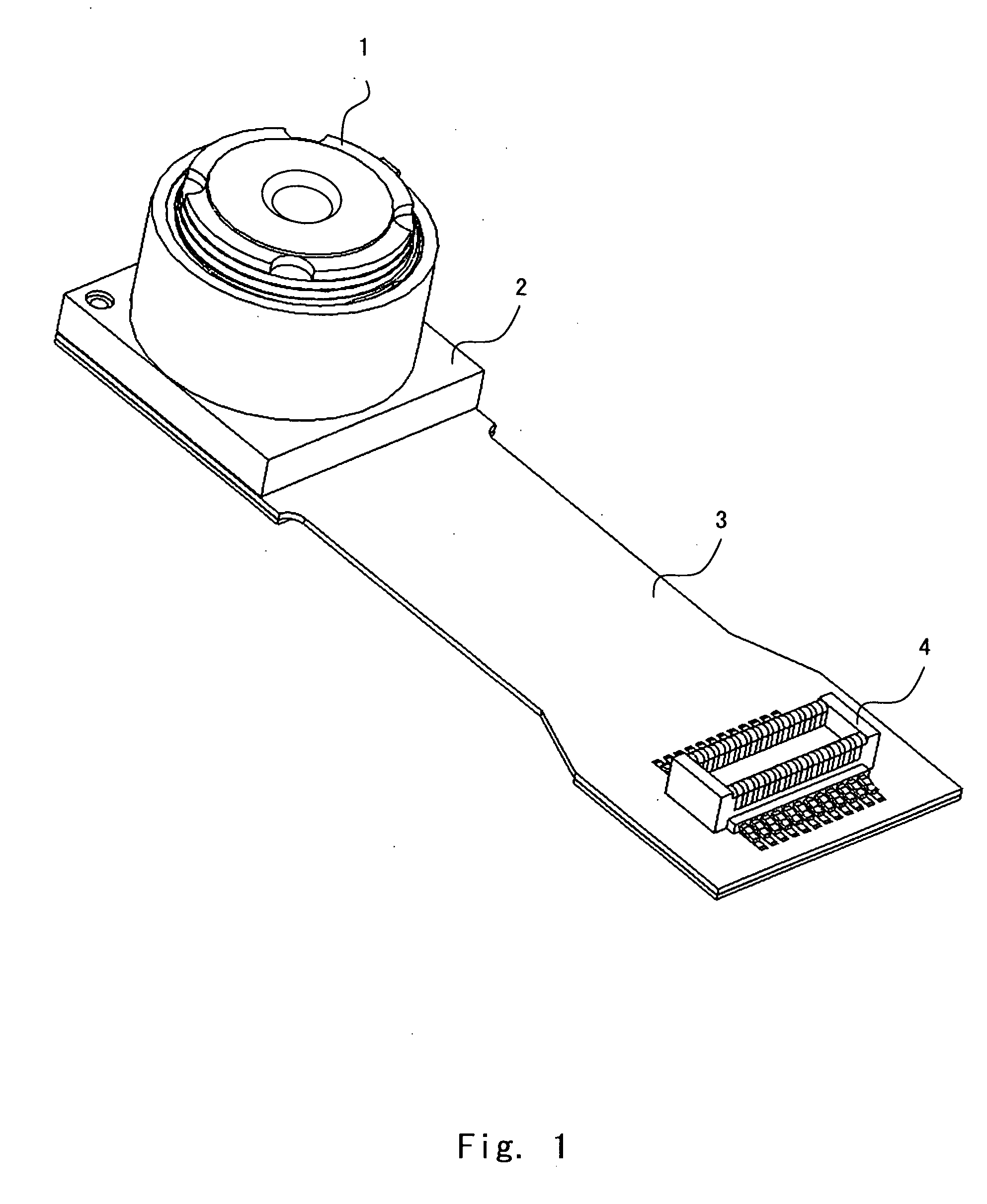
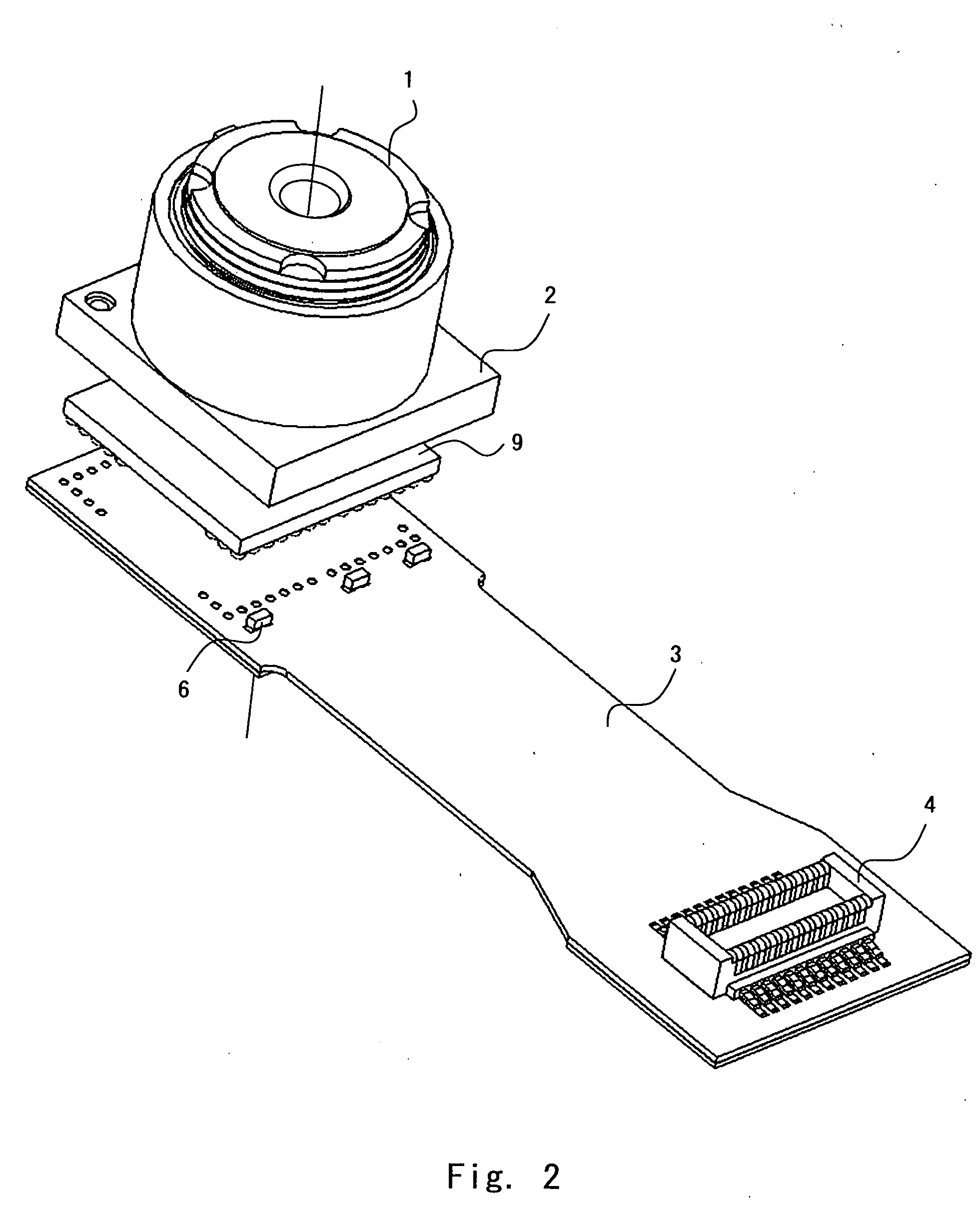
[0063]FIG. 1 is a perspective view showing the camera module according to the present invention. FIG. 2 is an exploded perspective view showing the camera module. Further, FIG. 3 is a cross-sectional diagram showing the camera module. As shown in FIGS. 1 to 3, the camera module of the present invention includes a lens module 1, a mount 2, a FPC (Flexible Printed Circuit) substrate 3, a connecter 4, a solid-state imaging device 5, a capacitor 6, a lens 7, an optical filter 8, a cover glass (cover plate) 9, a reinforcement sheet 10, and solder balls 11.
[0064]The lens module 1 is in a cylinder shape with one or more lenses accurately fixed to an inner peripheral surface thereof. Other than the lens 7, an optical aperture and an O ring may be provided in the lens module 1. A screw structure is provided on an outer peripheral surface of the lens module 1 so that it is screwed with the mount 2. The lens module 1 is formed of a synthetic resin with a light blocking effect such as a black p...
example 1
[0111]For a camera module of the first embodiment, the thickness of the lens holder 32 is created under the following condition. The configuration of the camera module is same as the one shown in FIG. 9.
S / (H×H)=0.1
example 2
[0112]For a camera module of the second embodiment, the thickness of the lens holder 32 is created under the following condition. The configuration of the camera module is same as the one shown in FIG. 9.
S / (H×H)=0.2
PUM
 Abstract
Description
Claims
Application Information