Method of fabrication and device configuration of asymmetrical DMOSFET with Schottky barrier source

a technology of asymmetrical dmosfet and barrier source, which is applied in the direction of semiconductor devices, semiconductor/solid-state device details, diodes, etc., can solve the problems of low drive current, subject to potential increased body bias, and limited conventional manufacturing processes, so as to achieve a much-reduced contact resistance

Active Publication Date: 2007-08-16
ALPHA & OMEGA SEMICON LTD
View PDF14 Cites 110 Cited by
  • Summary
  • Abstract
  • Description
  • Claims
  • Application Information

AI Technical Summary

Benefits of technology

[0009] Furthermore, this invention discloses a trench contact is formulated through mask and etching of the Schottky metal silicide at body contact region. This process provides a direct ohmic contact to the transistor body. Subsequent process steps eventually implement a metallization to contact the whole mesa region that includes the source and body contact. The metallization contact thus achieves a much-reduced contact resistance.

Problems solved by technology

However, conventional manufacturing processes are still limited by the use of metals of high barrier height.
The devices as now available to those of ordinary skill in the art therefore suffers low drive current and subject to potential increased body bias and reducing the gate drive or even forward bias the body-source junction and initiate a snapback.
However, the higher barrier height of the source contact can potentially increase the body bias and reduce the gate drive, or even increase the forward bias of the body-source junction and initiate a snapback.
For this reasons, the device suffers a low drive current.

Method used


Image

  • Method of fabrication and device configuration of asymmetrical DMOSFET with Schottky barrier source
  • Method of fabrication and device configuration of asymmetrical DMOSFET with Schottky barrier source
  • Method of fabrication and device configuration of asymmetrical DMOSFET with Schottky barrier source

Examples


Embodiment Construction

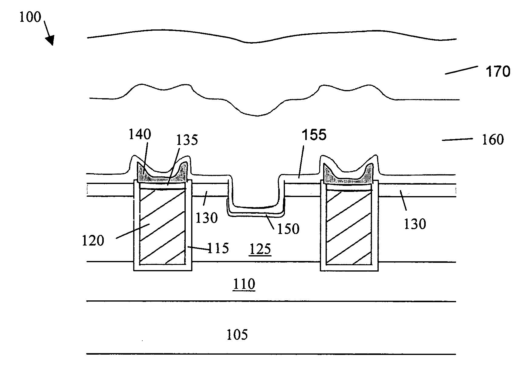
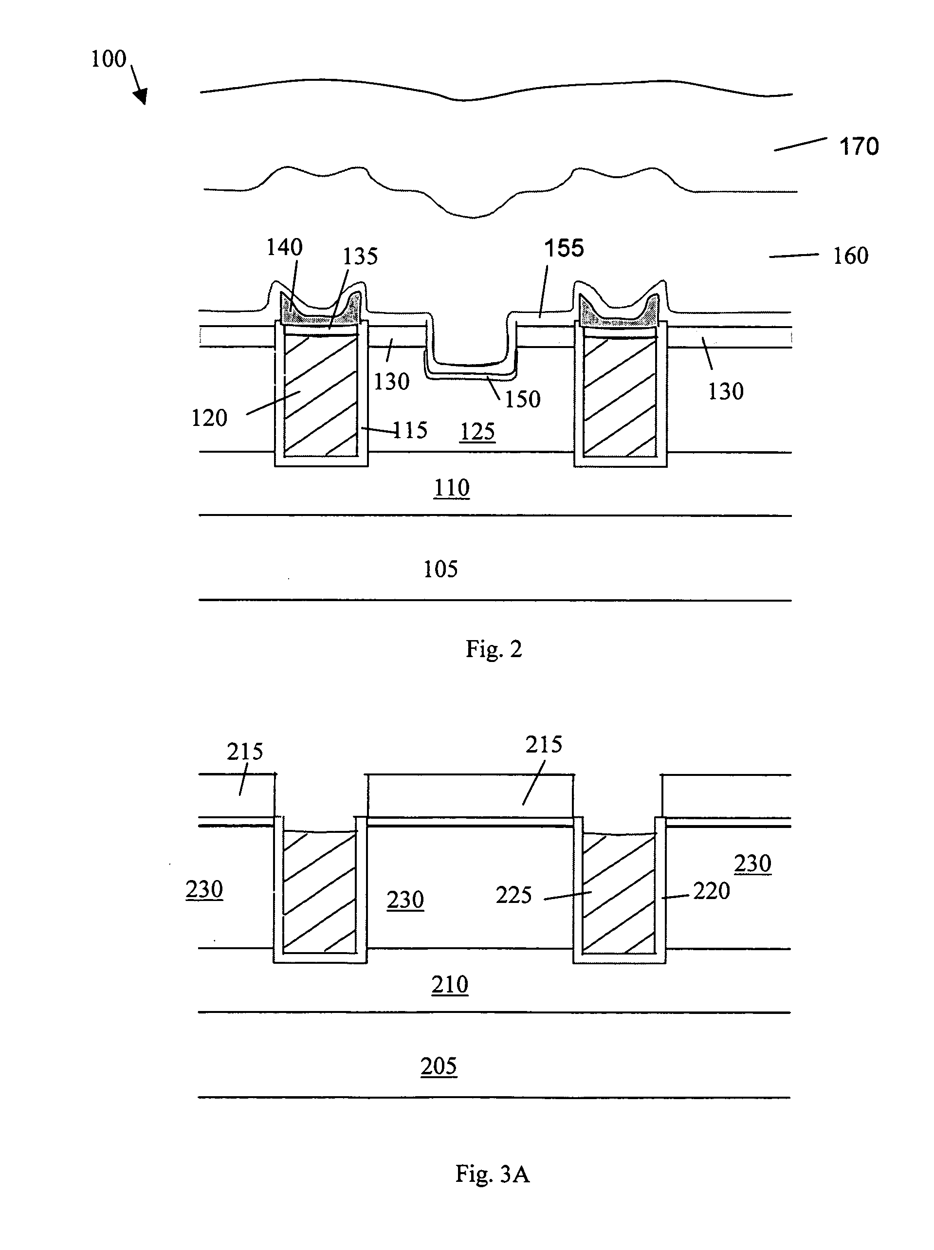
[0017] Referring to FIG. 2 for a cross sectional view of a trenched DMOS device 100. The trenched DMOS device 100 is supported on a substrate formed with an epitaxial drift layer 110. The DMOS device further includes a plurality of trenches opened in the epitaxial drift region 110. The trenches are padded with a gate oxide layer 115 and filled with a gate material, e.g., polysilicon 120. A body region 125 doped with a body dopant, e.g., P-type body dopant, surrounding the trenched gates 120. Encompassed in the body regions 125 are source regions 130 near the top surface of the epitaxial drift region 105 surrounding the trenched gates 120. The source region 130 is formed with a low barrier height metal to function as a silicide Schottky source. The gates 120 is insulated further from the source region with a top insulation oxide layer 135 covered under an insulated spacer, e.g., silicon nitride spacers 140, covering over the top oxide layer 135.

[0018] The DMOS device 100 further inc...


PUM


Abstract

A trenched semiconductor power device includes a trenched gate insulated by a gate insulation layer and surrounded by a source region encompassed in a body region above a drain region disposed on a bottom surface of a semiconductor substrate. The source region surrounding the trenched gate includes a metal of low barrier height to function as a Schottky source. The metal of low barrier height further may include a PtSi or ErSi layer. In a preferred embodiment, the metal of low barrier height further includes an ErSi layer. The metal of low barrier height further may be a metal silicide layer having the low barrier height. A top oxide layer is disposed under a silicon nitride spacer on top of the trenched gate for insulating the trenched gate from the source region. A source contact disposed in a trench opened into the body region for contacting a body-contact dopant region and covering with a conductive metal layer such as a Ti / TiN layer. In a preferred embodiment, the semiconductor power device constitutes an asymmetrical double diffusion metal oxide semiconductor field effect transistor (DMOSFET) device.

Description

BACKGROUND OF THE INVENTION [0001] 1. Field of the Invention [0002] The invention relates generally to the semiconductor power devices. More particularly, this invention relates to an improved and novel device manufacturing process to provide asymmetrical double diffusion metal oxide semiconductor field effect transistor (DMOSFET) with Schottky barrier source implemented with low-barrier height rare earth metal silicide for a best drive current without subject to a limitation of the high temperature processes and meanwhile providing low contact resistance of source and body contacts, which is achieved through silicided contact on the entire mesa area totally insulated from the trenched gates covered under an insulated spacer. [0003] 2. Description of the Prior Art [0004] It is known in the semiconductor power industry to implement a Schottky barrier source or metal silicide source electrode to overcome the parasitic bipolar conduction in a DMOSFET device. In order to prevent an uncl...

Claims


Application Information

Patent Timeline
Patent Type & Authority Applications(United States)
IPC IPC(8): H01L29/94
CPCH01L29/41766H01L29/456H01L29/66727H01L29/66734H01L29/7806H01L2924/0002H01L29/7813H01L29/7839H01L2924/00H01L21/28518H01L21/823418H01L29/665H01L29/66507H01L29/7845
Inventor HU, YONGZHONGTAI, SUNG-SHAN
Owner ALPHA & OMEGA SEMICON LTD
Why Eureka
Try Eureka