Customizable power and ground pins

a technology of power and ground pins, which is applied in the direction of semiconductor devices, semiconductor/solid-state device details, electrical apparatuses, etc., can solve the problems of limiting the logical function, the bouncing of power and ground rings, and aggravating the already problematic power and ground noise. , to achieve the effect of reducing the noise produced

Inactive Publication Date: 2007-08-16
INTEL CORP
View PDF23 Cites 12 Cited by
  • Summary
  • Abstract
  • Description
  • Claims
  • Application Information

AI Technical Summary

Benefits of technology

[0008] Embodiments of the current invention, in addition to providing a set of single via customizable components, also provide single via customizable power and ground connections within the I / O cells. Depending on the packaging options, the bonded but unused I / O sites may be customized as power or ground pins, or unused I / O sites that are customized as power or ground pins may be custom bonded either to power / ground planes in the package or directly to package pins, as needed to minimize the noise produced by the simultaneously switching output buffers.

Problems solved by technology

The advantages of such application-specific integrated circuits (ASICs) have been clearly defined in the prior art, but are limited to logical functions.
These devices switch large amounts of current, which causes their power and ground rings to bounce.
All of this results in longer wire bonds between the chip and the package, which have more inductance, further aggravating the already problematic power and ground noise caused by the faster switching speeds of the high speed output devices.
Field-programmable gate arrays (FPGAs), on the other hand, have a fixed arrangement of such power and ground pins, and therefore must limit the chip designer's use of adjacent simultaneously switching outputs, and cannot provide the alternative of adding additional power and ground pins.

Method used


Image

  • Customizable power and ground pins
  • Customizable power and ground pins
  • Customizable power and ground pins

Examples


Embodiment Construction

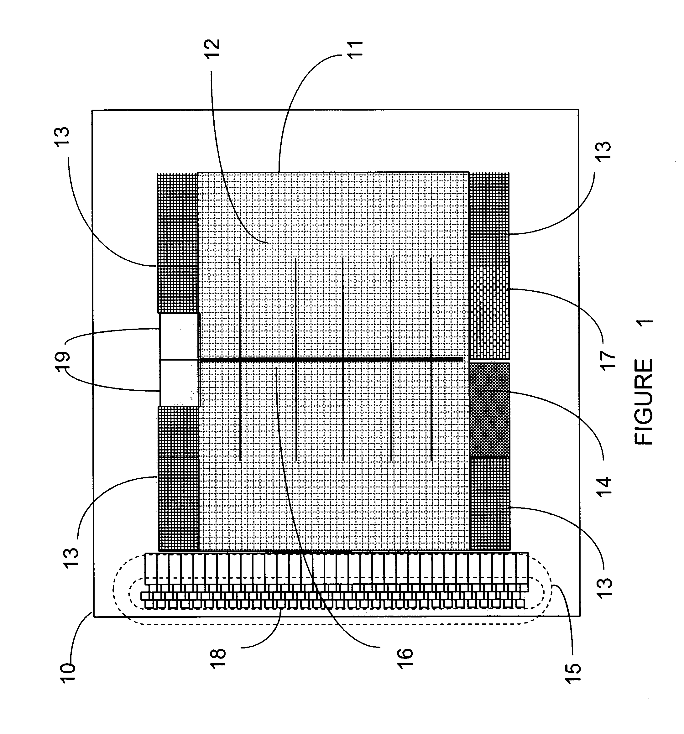
[0022] Reference is now made to FIG. 1, which is a simplified illustration of a personalizable and programmable integrated circuit device 10 constructed and operative in accordance with a preferred embodiment of the present invention. The device contains four groups of customizable I / O buffers 15, each with three tiers of I / O pads 18.

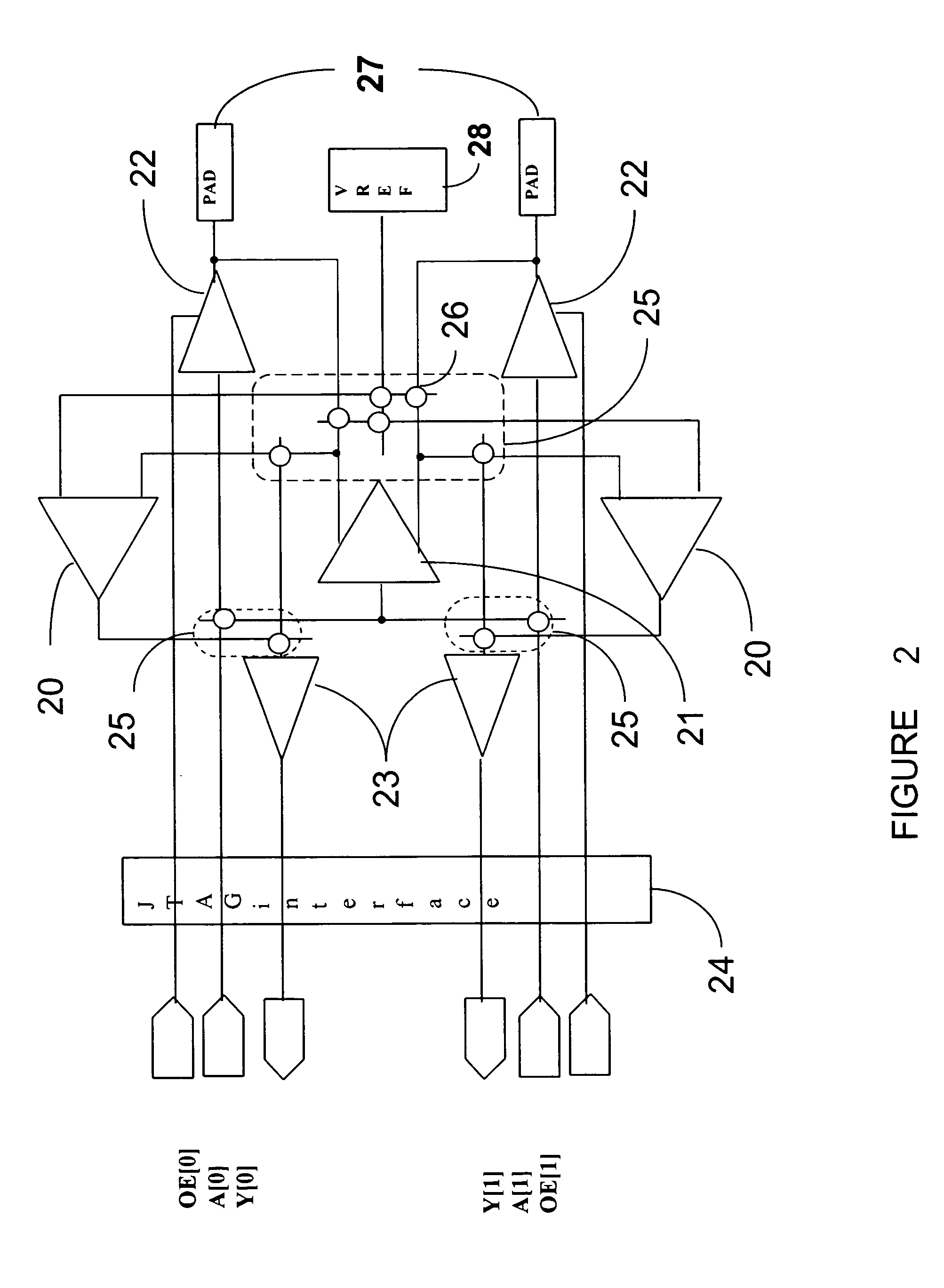
[0023] Reference is now made to FIG. 2, an illustration of a customizable I / O buffer. Each I / O buffer has two pads 27, each of which may be customized to be used as an input or output pad, and one pad 28, which may be customized to be used as a voltage reference pad. While this example has two pads 27, a customizable I / O buffer with a single pad, which may be customized to be used as an input or output pad, may be constructed.

[0024] Reference is now made to FIG. 3, an illustration of the physical power and ground connections within a customizable I / O cell. When unused, each of the pads 30, 31 and 37 may be connected directly to either the internal pow...


PUM


Abstract

A configurable logic array composed of: a multiplicity of logic cells, each containing look-up tables, a multiplicity of customizable I / O cells, each containing a multiplicity of pads; and a customizable via connection layer for customizing the cells and interconnect between them, may be constructed to include the option of customizing the I / O cells to act as power or ground pins. Assigning custom power and ground pins may depend on the types of I / O cells and package bonding options.

Description

FIELD OF THE INVENTION [0001] The present invention relates to integrated circuit devices as well as to methods for personalizing the power and ground connections to such devices. BACKGROUND OF THE INVENTION [0002] The following U.S. patent applications and granted patents are believed to represent the current state of the art: U.S. Pat. Nos. 5,898,225, 6,015,723, 6,331,733, 6,245,634, 6,819,229, 6,194,912 and application Ser. No. 10 / 899,020. [0003] The above patents describe semiconductor devices, which contain logic cells that further contain look up tables and interconnects, which may be patterned by a single via mask. The advantages of such application-specific integrated circuits (ASICs) have been clearly defined in the prior art, but are limited to logical functions. Today, most semiconductor devices also comprise numerous high-speed output devices. These devices switch large amounts of current, which causes their power and ground rings to bounce. In addition, the increasingly...

Claims


Application Information

Patent Timeline
Patent Type & Authority Applications(United States)
IPC IPC(8): H01L23/02
CPCH01L23/50H01L2924/01033H01L2224/48091H01L2224/49109H01L2224/49113H01L2924/01002H01L2924/01005H01L2924/01057H01L2924/14H01L2924/1433H01L2924/15153H01L2924/1517H01L2924/15312H01L2924/30107H01L24/49H01L2924/01006H01L24/48H01L2924/00014
Inventor MIHELCIC, STAN J.LEVINTHAL, ADAMCOOKE, LAURENCE H.
Owner INTEL CORP
Why Eureka
Try Eureka