Fast read port for register file

a register file and read port technology, applied in information storage, static storage, digital storage, etc., can solve the problems of increasing the size and complexity of the overall memory array of pullup stack replication, and achieve the effect of low input loading, minimal likelihood of upsetting the data content of memory cells, and rapid read respons

Inactive Publication Date: 2007-08-16
ATMEL CORP
View PDF12 Cites 30 Cited by
  • Summary
  • Abstract
  • Description
  • Claims
  • Application Information

AI Technical Summary

Benefits of technology

[0010] Separate read and write ports in a memory system allow simultaneous access to a memory cell array in read and write operations. A single cycle operation of a central processing unit coupled to a memory cell array depends on a memory access capability incorporating simultaneous read and write operations. A pair of pull-down transistor stacks coupled to a memory cell latch loop allow a selected single pull-down stack of the pair to toggle the memory cell latch loop to a desired data content without any requirement for a precharge scheme. An additional single pull-down stack of transistors connected to a memory cell latch loop provides a read port with low input loading and minimal likelihood of upsetting a memory cell data content in a read operation. A sense amplifier provides a mid-supply-level precharge capability produced by a feedback device within a front-end inversion stage. The front-end inversion stage, cascaded with a second inversion stage, provides a rapid read response. A memory cell of the present invention may be used for a register file, a specialized SRAM, or a generic SRAM.

Problems solved by technology

The pullup stack replication increases an overall memory array size and complexity.

Method used


Image

  • Fast read port for register file
  • Fast read port for register file
  • Fast read port for register file

Examples


Embodiment Construction

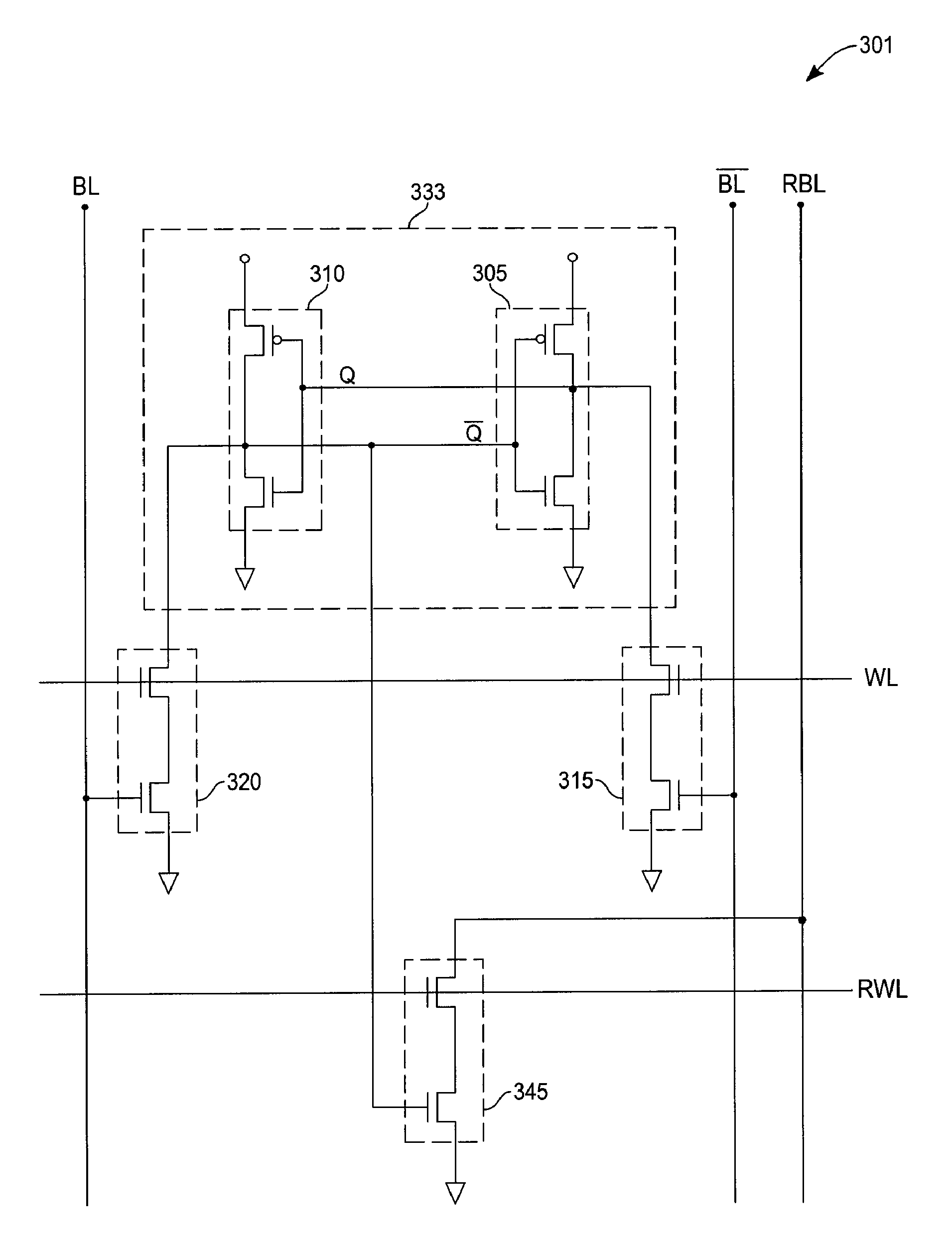
[0024] With reference to FIG. 3A, a first CMOS inverter 305 is cross-coupled with a second CMOS inverter 310 in an exemplary schematic diagram of a static memory cell 301. The first and second CMOS inverters 305, 310 form a memory cell latch loop 333 of a static RAM cell. A first output of the memory cell latch loop Q and a second output of the memory cell latch loop Q are formed by the outputs of the first and second CMOS inverters 305, 310 respectively. The first output of the memory cell latch loop Q connects to an output drain of a first two-transistor stack 315. The second output of the memory cell latch loop Q connects to an output drain of a second two-transistor stack 320. The second output of the memory cell latch loop Q also connects to a data input of a third two-transistor stack 345. The first, second, and third two-transistor stacks 315, 320, 345 are shown, for example, as a series connection of NMOS transistors with common source-drain diffusion and conductive channels...


PUM


Abstract

Separate read and write ports in a memory system allow simultaneous access to a memory cell array by read and write operations. A single cycle operation of a central processing unit coupled to a memory array depends on a memory access capability providing simultaneous reading and writing to different locations. A pair of pull-down transistor stacks connected to memory cell latch loops allows a single selected pull-down stack of the pair to toggle a memory cell latch loop to a desired data content without any requirement for a precharge scheme. A single pull-down stack of transistors connected to a memory cell latch loop provides a read port with low input loading. A sense amplifier provides a mid-supply-level precharging capability provided by a feedback device within a front-end inversion stage. When not in a feedback mode, the front-end inversion stage cascaded with a second inversion stage provides a rapid read response.

Description

CROSS-REFERENCE TO RELATED APPLICATION [0001] This is a divisional of pending U.S. patent application Ser. No. 11 / 130,929; filed May 17, 2005.TECHNICAL FIELD [0002] The invention relates to memory systems and read operations. More specifically, the invention is a single-ended read port and sense amplifier with integral precharge capability. BACKGROUND ART [0003] A static memory cell constructed from six transistors is commonly applied in memory designs to fulfill requirements for short access cycle times, high-frequency data rates, low power consumption, and excellent immunity from extreme environmental conditions. [0004] With reference to FIG. 1A a six transistor (6-T) cell latches digital data in a memory cell latch loop formed by a pair of cross-coupled inverters in a prior art static memory cell diagram 101. A first complementary inverter is constructed from a first PMOS transistor 115 and a first NMOS transistor 125. A second complementary inverter is constructed from a second ...

Claims


Application Information

Patent Timeline
Patent Type & Authority Applications(United States)
IPC IPC(8): G11C8/00
CPCG11C11/413G11C8/00
Inventor LAMBRACHE, EMILFROEMMING, BENJAMIN F.
Owner ATMEL CORP
Why Eureka
Try Eureka