Soldering structure of through hole

a technology of through hole and structure, which is applied in the direction of printed circuit manufacturing, printed circuit aspects, cooking vessels, etc., can solve the problems of defective soldering, so-called insufficient solder rise, and solder not sufficiently rising above the upper face of the through hole, so as to achieve the effect of improving the soldering performan

Inactive Publication Date: 2007-09-06
KK TOKAI RIKA DENKI SEISAKUSHO
View PDF3 Cites 2 Cited by
  • Summary
  • Abstract
  • Description
  • Claims
  • Application Information

AI Technical Summary

Benefits of technology

[0007] The invention has been made in view of the above described circumstance, and it is an object of the invention to provide a soldering structure of a through hole in which soldering performance can be improved, even in case where an electronic component having a lead terminal is soldered to a through hole formed in a printed board by means of a lead free solder.

Problems solved by technology

However, there is a tendency that the eutectic solder as described above is not used in respect of environmental pollution, and a lead free solder has come to be used instead of the eutectic solder.
Because the lead free solder has a higher melting point as compared with the eutectic solder, a so-called insufficient solder rise may occur.
Specifically, when the printed board is taken out from the bath of molten solder, the solder has not sufficiently risen above an upper face of the through hole.
Consequently, there has been a trouble that defective soldering may occur.
Because the lead free solder 5, has a higher melting point as compared with the eutectic solder of Sn—Pb, as described above, the solder rise will be insufficient when heat conduction is poor.
However, in case where the multilayer printed board 1 has been dipped in the bath of solder for a long time for the purpose of enhancing the heat conduction thereby to improve the solder rise, thermal damage would be given to the electronic component and the printed board to be soldered, to the contrary.
Therefore, this is not a favorable solution, practically.
For this reason, soldering had better be conducted for an allowable maximal dipping time, which however, will also cause an insufficient solder rise, and there has been probability that soldering performance may be deteriorated.

Method used


Image

  • Soldering structure of through hole
  • Soldering structure of through hole
  • Soldering structure of through hole

Examples


Embodiment Construction

[0016] Now, an embodiment of the invention will be described referring to FIGS. 1 to 3.

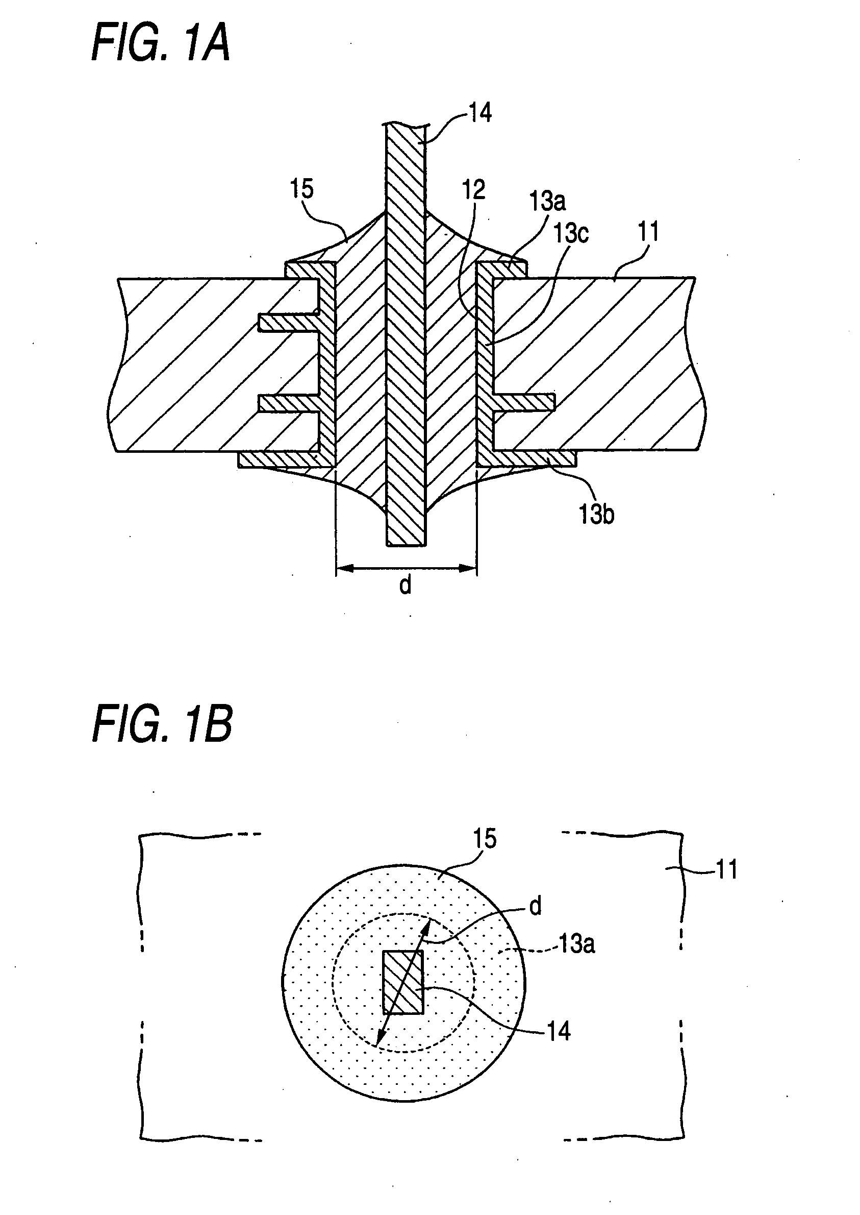
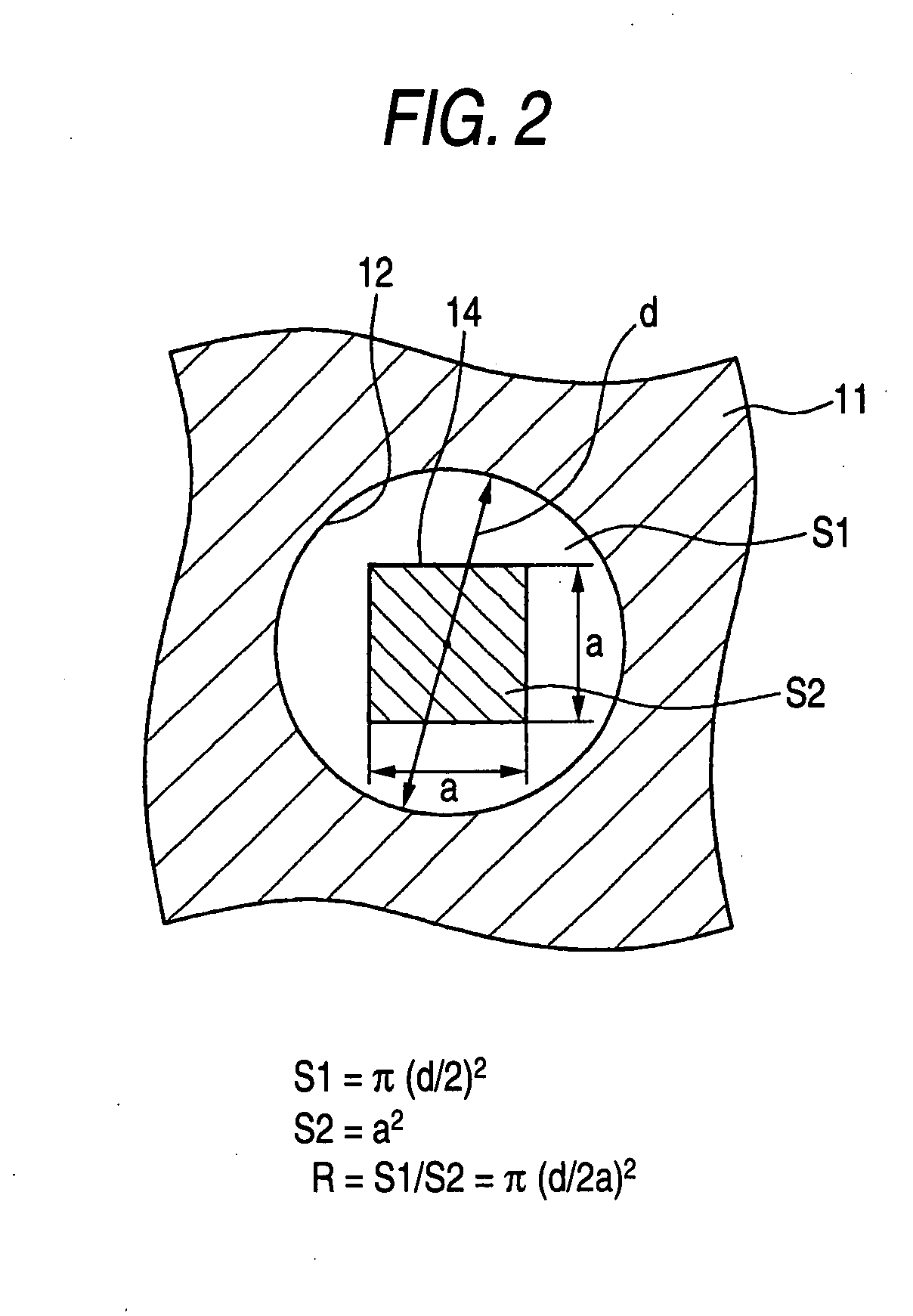
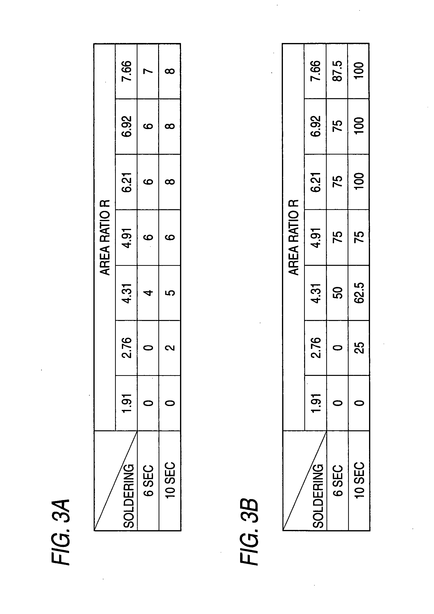
[0017]FIGS. 1A and 1B are a sectional view and a plan view showing the embodiment. A multilayer printed board 11 includes a plurality of wiring layers stacked on one another. Conductor patterns for wiring are formed on both an upper face and a lower face of the multilayer printed board 11, and other conductor patterns for wiring are also formed in inner intermediate layers thereof. A through hole 12 for mounting an electronic component is formed in an illustrated part. Conductor patterns 13a and 13b are formed on the upper face and the lower face of the multilayer printed board 11 in such a manner that the upper and lower conductor patterns 13a, 13b are electrically connected to each other, by means of a through hole soldering part 13c.

[0018] The through hole 12 is formed for the purpose of inserting the electronic component therein. A lead terminal 14 of the electronic component is inserted int...


PUM


Abstract

A through hole is formed in a printed board. Conductor patterns are formed on an upper face and a lower face of the printed board in such a manner that the conductor patterns are electrically connected to each other, by means of a through hole solder. A lead terminal of an electronic component is inserted into the through hole and soldered with a lead free solder. According to this invention, an area of an opening of the through hole is set to be four times or more as large as a cross sectional area of the lead terminal. In this manner, heat conduction on occasion of soldering can be enhanced, and the soldering can be favorably performed, even when the lead free solder having a high melting point is used.

Description

BACKGROUND OF THE INVENTION [0001] The present invention relates to a soldering structure of a through hole in which a lead terminal of an electronic component is soldered to a through hole formed in a printed board, using a lead (Pb) free solder. [0002] In case where an electronic component provided with a lead terminal is mounted on a printed board by forming a through hole therein, the printed board in a state having the lead terminal inserted into the through hole will be dipped in a bath of molten solder, thereby to fill the solder in the through hole. Generally, in this case, when a eutectic solder (Sn—Pb solder) is used, an opening area of the through hole is set to be about twice as large as a cross sectional area of the lead terminal. No document will be particularly referred to, because mounting of a component on a printed board in this manner belongs to general technique. [0003] However, there is a tendency that the eutectic solder as described above is not used in respec...

Claims


Application Information

Patent Timeline
Patent Type & Authority Applications(United States)
IPC IPC(8): A47J36/02
CPCH05K3/3447H05K2201/09854H05K3/3463
Inventor SUZUKI, NORIHITOMINOURA, AKIHIRO
Owner KK TOKAI RIKA DENKI SEISAKUSHO
Why Eureka
Try Eureka