

Data recording method of semiconductor integrated circuit device
a data recording and integrated circuit technology, applied in the field of data recording systems of semiconductor integrated circuit devices, can solve the problems of slow data writing and reading, inferior write speed and read speed of recording media,
- Summary
- Abstract
- Description
- Claims
- Application Information
AI Technical Summary
Benefits of technology
Problems solved by technology
Method used
Image

Examples
first embodiment
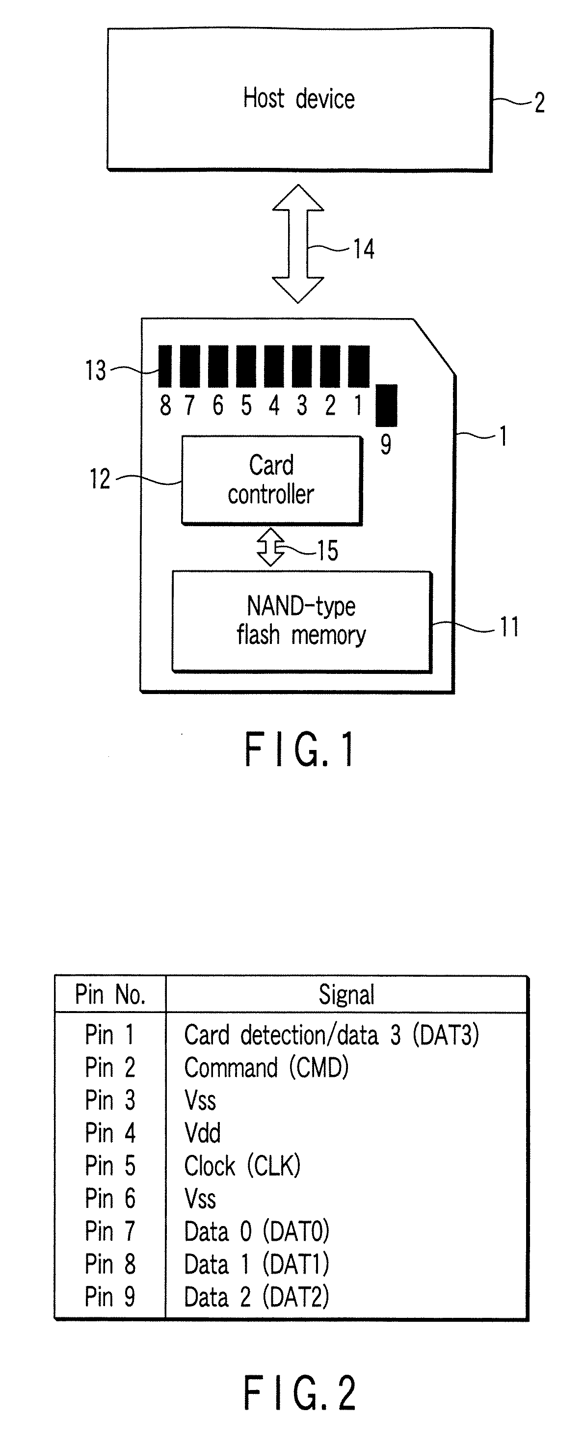
[0027]FIG. 1 is a view showing an example of a memory card.
[0028] As shown in FIG. 1, a memory card 1 transmits data to and receives data from a host device 2 via a bus interface 14. The memory card 1 is formed to be removable from a slot provided in the host device 2.
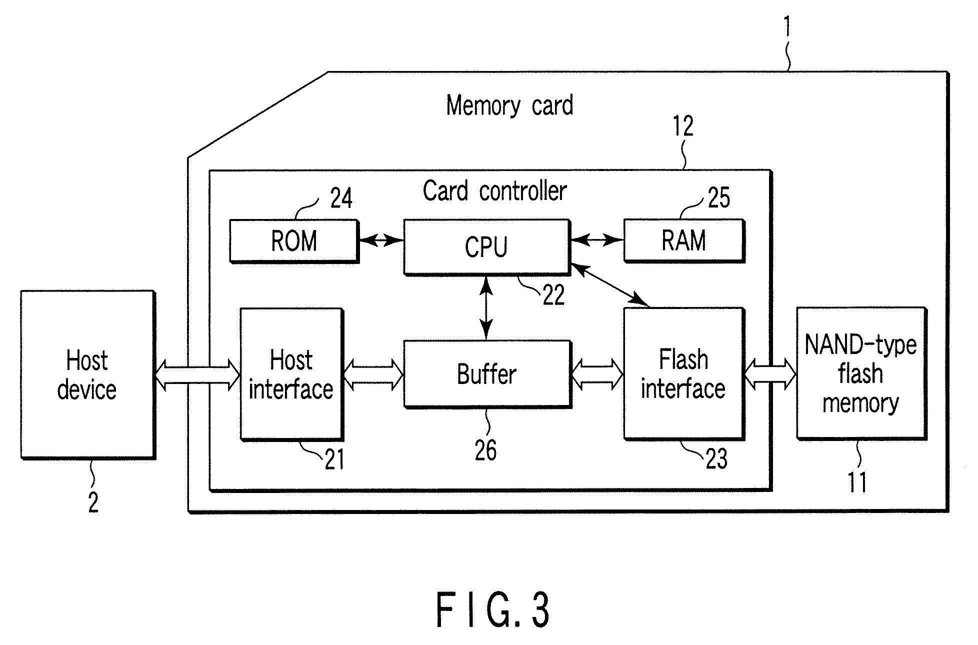
[0029] The memory card 1 comprises a NAND-type flash memory 11; a card controller 12 that controls this flash memory 11; and a plurality of signal pins (first to ninth pins) 13.
[0030] The signal pin 13 serves as a pin electrically connected to the card controller 12, and functions as an external pin of the memory card 1. FIG. 2 shows an example of assignment of signals with respect to the first to ninth pins in the signal pin 13.
[0031] As shown in FIG. 2, data 0 to data 3 are assigned to a seventh pin, an eighth pin, a ninth pin, and a first pin, respectively. The first pin is assigned to a card detection signal as well as data 3. Further, the second pin is assigned to a command; the third pin and the sixth pin eac...
second embodiment
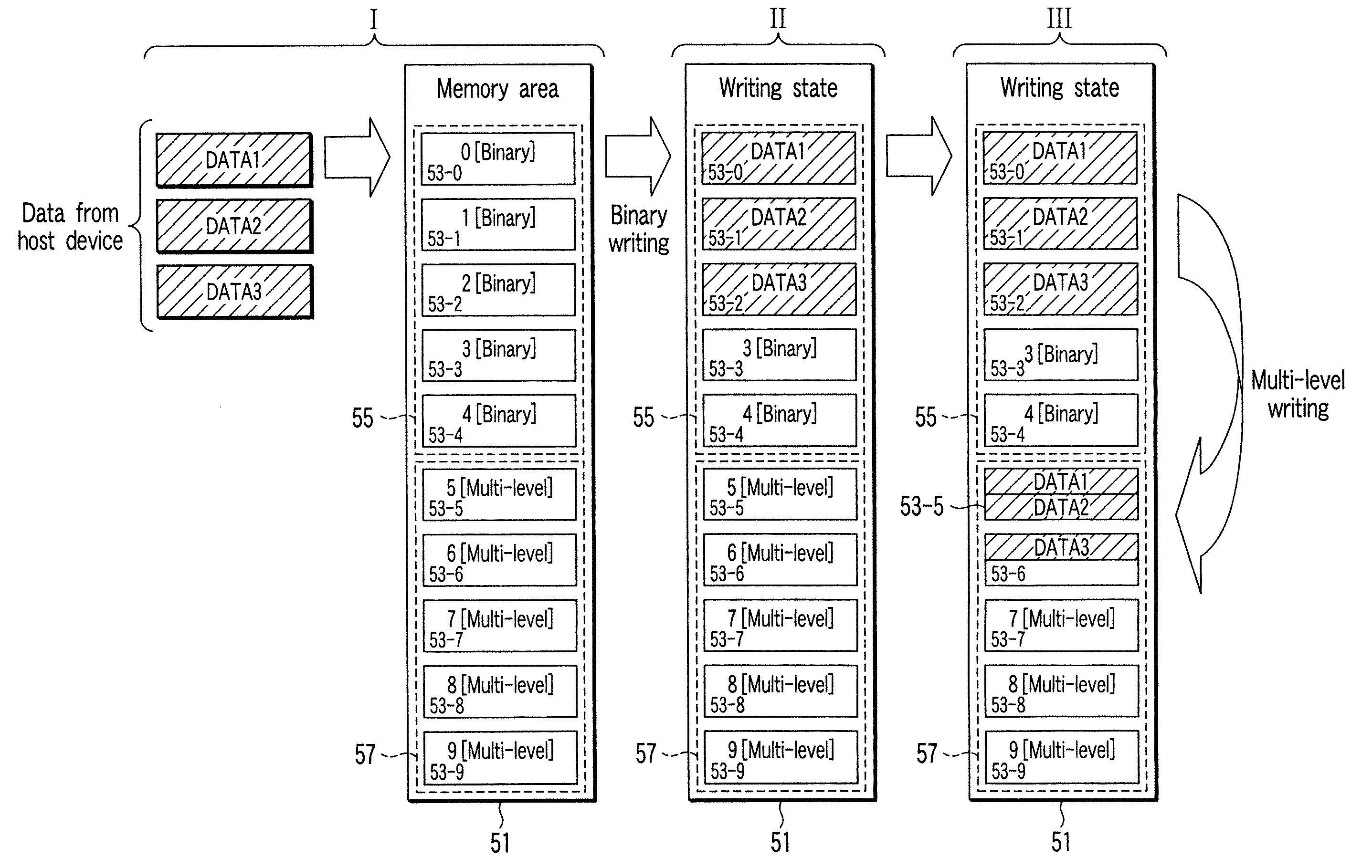
[0079] A second embodiment is an example relating to an operating state in the case where the available space of a binary area 55 is reduced.
[0080]FIG. 8 is a view showing a data recording system of a NAND-type flash memory according to the second embodiment of the present invention.
[0081] As shown in state IV of FIG. 8, assume that data (DATA 4 to DATA 6) for three unit areas has been sent from a host device 2. At this time, as shown in state V, assume that only two unit areas 53-3 and 53-4 are provided as available spaces of the binary area 55. In this case, there occurs shortage of one unit area.
[0082] When available space is eliminated from the binary area 55, in the second embodiment, the data transmitted from the host device 2 is recorded in an overwritten manner in a portion at which the data copied to a multi-level area 57 exists among the data recorded in the binary area 55.
[0083] The available spaces of the binary area 55 of the present example are two unit areas, the ...
third embodiment
[0086] A third embodiment presents an example relating to an operating state in the case where the available space of a multi-level area 57 is reduced.
[0087]FIG. 9 is a view showing a data recording system of a NAND-type flash memory according to the third embodiment of the present invention.
[0088] As shown in state VIII of FIG. 9, assume that available space does not exist in the multi-level area 57. When no available space is left in the multi-level area 57, a binary area 55 is partially changed to the multi-level area 57, as shown in state IX, in the third embodiment.
[0089] In unit areas 53-5 to 53-9 of the multi-level area 57, data (DATA 1 to DATA 10) is recorded as shown in states VIII and IX, and no available space exists. Therefore, in the present example, among unit areas 53-0 to 53-4 of the binary area 55, the three unit areas 53-2 to 53-4 are changed from the binary area 55 to the multi-level area 57. Data (DATA 8 to DATA 10) is recorded in these three unit areas 53-2 t...
PUM
 Abstract
Description
Claims
Application Information