
Non-volatile memory and method with multi-stream updating

a non-volatile memory and multi-stream updating technology, applied in the direction of memory architecture accessing/allocation, instruments, computing, etc., can solve the problems of erroneous data to be read, storage level shift, less than optimal wear leveling, etc., to improve the performance of the memory system, improve the degree of parallelism, and efficiently write

Active Publication Date: 2006-07-13
SANDISK TECH LLC
View PDF75 Cites 149 Cited by
  • Summary
  • Abstract
  • Description
  • Claims
  • Application Information

AI Technical Summary

Benefits of technology

[0163] The same host writes example in FIG. 24 and FIG. 25 will be used to illustrate the advantage of the invention shown in FIG. 27A. In host write #1, the command is to write LS10′. Since LS10′ should occupy slot 3, a full page could not be written to the update block 20. Instead, it is staged by being buffered in a new page of the SPB 30. Thus, LS10′ is stored in slot 3 of the next available partial page PP0 of the SPB 30. At the same time, slots 1 and 2 are optionally padded with LS8 and LS9 respectively. Also, according to the feature of the invention, both the SPBI and the CBI are packaged within a sector, namely, an index sector SPBI / CBI1 50, and the index sector 50 is advantageously stored in the last, unused slot of the partial page PP0.
[0164] In host write #2, the command is to write LS11′. Since LS11′ belongs to slot 4, which is at a page end, a full page pre-padded with sequential LS8, LS9 and LS10′ from the SPB 30 can be written to the next available page P0 of the update block 20. In this case, the index sector for SPBI / CBI is not updated since it is not writing to a partial page in the SPB 30. Alignment, as well as pre-padding in SPB is preferred but optional.
[0165] In host write #3, the command is to write LS6′ and LS7′. They belong to slots 3 and 4 respectively. Thus, another full page, P1 of the update block 20 is written when the preceding slots are padded with LS4 and LS5. Again, the index sector for SPBI / CBI is not updated since it is not writing to a partial page in the SPB 30.
[0166] In host write #4, the command is to write LS10″. Since LS10″ belong to slot 3, it will be written to the next partial page PP1 of the SPB 30. Similarly, the preceding slots 1 and 2 are padded with LS8 and LS9, while the last slot will also be stored with the latest update of the index sector, SPBI / CBI3.
[0167] The scheme shown in FIG. 27A is a more efficient utilization of the update block as evident from comparing the usage of the update block 20 at the end of host write #4 with that of FIG. 25. For the same host writes, the scheme shown in FIG. 27A consumes less storage and requires less padding in the update block, albeit at the expense of the scratch pad block 30. At the same time, the indexing scheme takes advantage of the unused storage in the scratch pad block to store an index in nonvolatile memory.
[0168] One important feature and advantage of the invention is that sequential order of update sectors in the update block is maintained during a series of separate host writes of sequential logical sectors, unlike the example shown in FIG. 25. This will be evident from the example illustrated in FIG. 27B.

Problems solved by technology

Zones are primarily used to simplify address management such as logical to physical translation, resulting in smaller translation tables, less RAM memory needed to hold these tables, and faster access times to address the currently active region of memory, but because of their restrictive nature can result in less than optimum wear leveling.
These storage levels do shift as a result of charge disturbing programming, reading or erasing operations performed in neighboring or other related memory cells, pages or blocks.
Also, shifting charge levels can be restored back to the centers of their state ranges from time-to-time, before disturbing operations cause them to shift completely out of their defined ranges and thus cause erroneous data to be read.
Once the page has been written, no further writing may be possible without corrupting the data that is already written.
Such memory arrays may be inefficiently programmed where data is received in amounts that are less than the size of a page.
Thus, the sectors are stored in a way that is inefficient in how it uses space in the memory array.
The programming of the second page of data may cause corruption of the first page of data in some cases.
Where parallelism of less than a page is used, space in the memory array may be wasted and this wasted space means that garbage collection must be performed more often thus adversely affecting the efficiency of the memory system.

Method used


Image

  • Non-volatile memory and method with multi-stream updating
  • Non-volatile memory and method with multi-stream updating
  • Non-volatile memory and method with multi-stream updating

Examples


embodiment

Scratch-Pad-Block Write Pointer Embodiment

[0240] According to another embodiment of the invention, synchronization information is maintained that would allow determination of whether a given logical sector buffered in the scratch pad block has been rendered obsolete by subsequent writes to the update block. This is accomplished by including a scratch-pad write pointer that gives the address of the location for the next write in the scratch pad block at the time the synchronization information is stored in a page of the update block.

[0241]FIG. 35A and FIG. 35B shows the intermediate state of the scratch pad block and the update block relative to the scratch-pad write pointer respectively after the successive host writes of FIG. 33A and FIG. 33B.

[0242]FIG. 35A illustrates the state of the scratch pad block and the update block after host write #1. In host write #1, the logical sector LS10′ belongs to slot 3 of the page and not at a page boundary and is therefore recorded in a partia...


PUM


Abstract

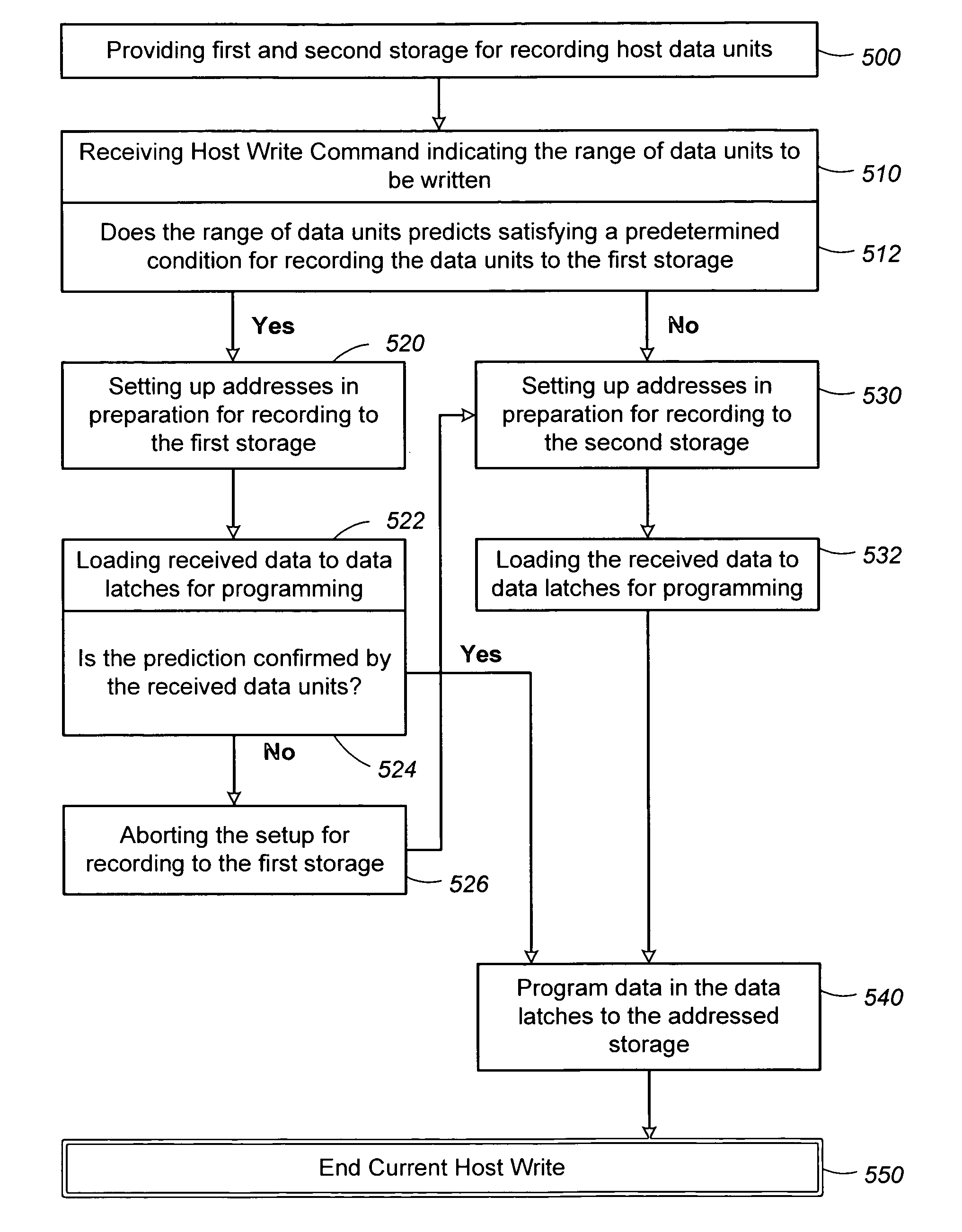
In a memory that is programmable page by page and each page having multiple sectors that are once-programmable, even if successive writes are sequential, the data recorded to an update block may be fragmented and non-sequential. Instead of recording update data to an update block, the data is being recorded in at least two interleaving streams. When a full page of data is available, it is recorded to the update block. Otherwise, it is temporarily recorded to the scratch pad block until a full page of data becomes available to be transferred to the update block. Preferably, a pipeline operation allows the recording to the update block to be set up as soon as the host write command indicates a full page could be written. If the actual write data is incomplete due to interruptions, the setup will be canceled and recording is made to the scratch pad block instead.

Description

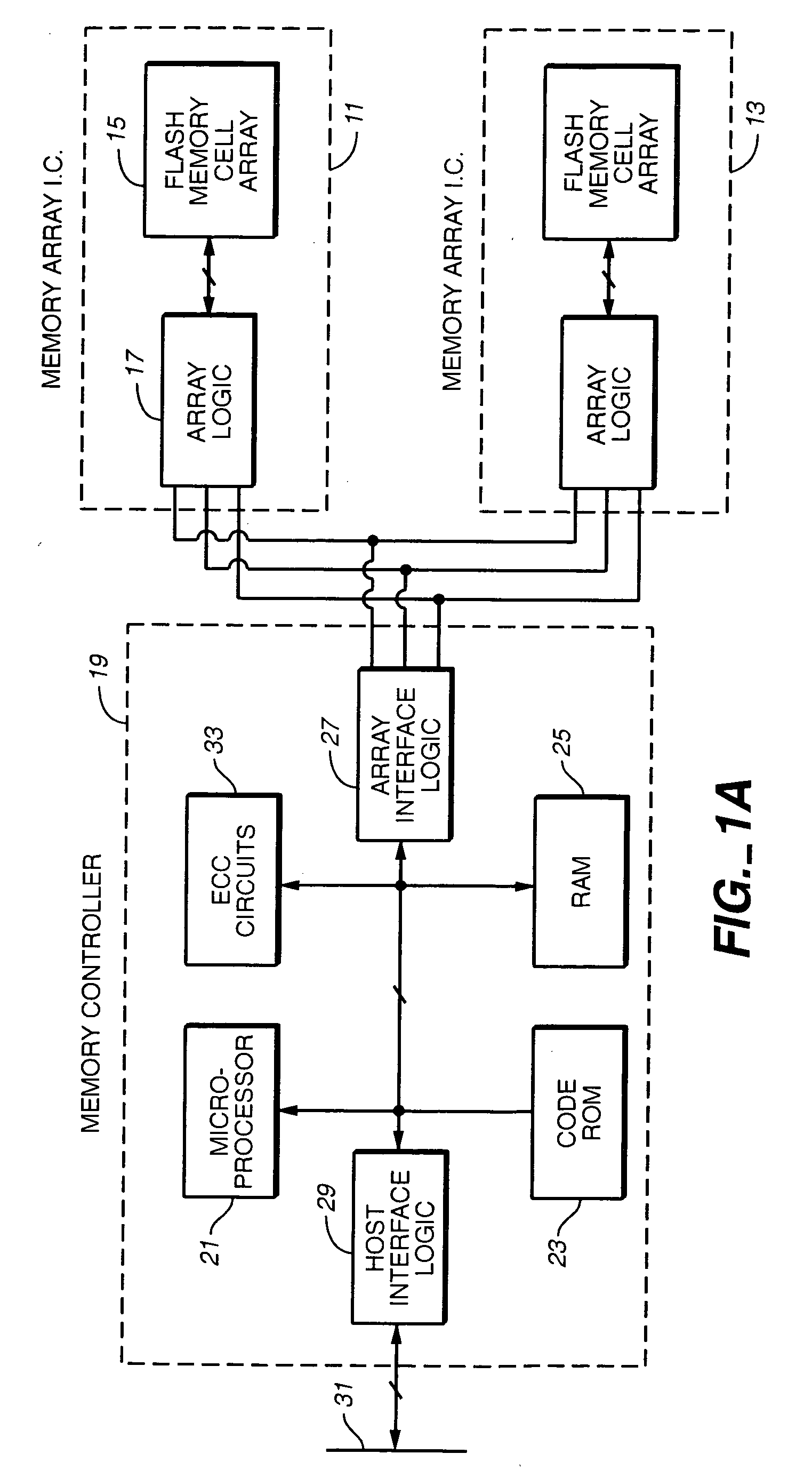
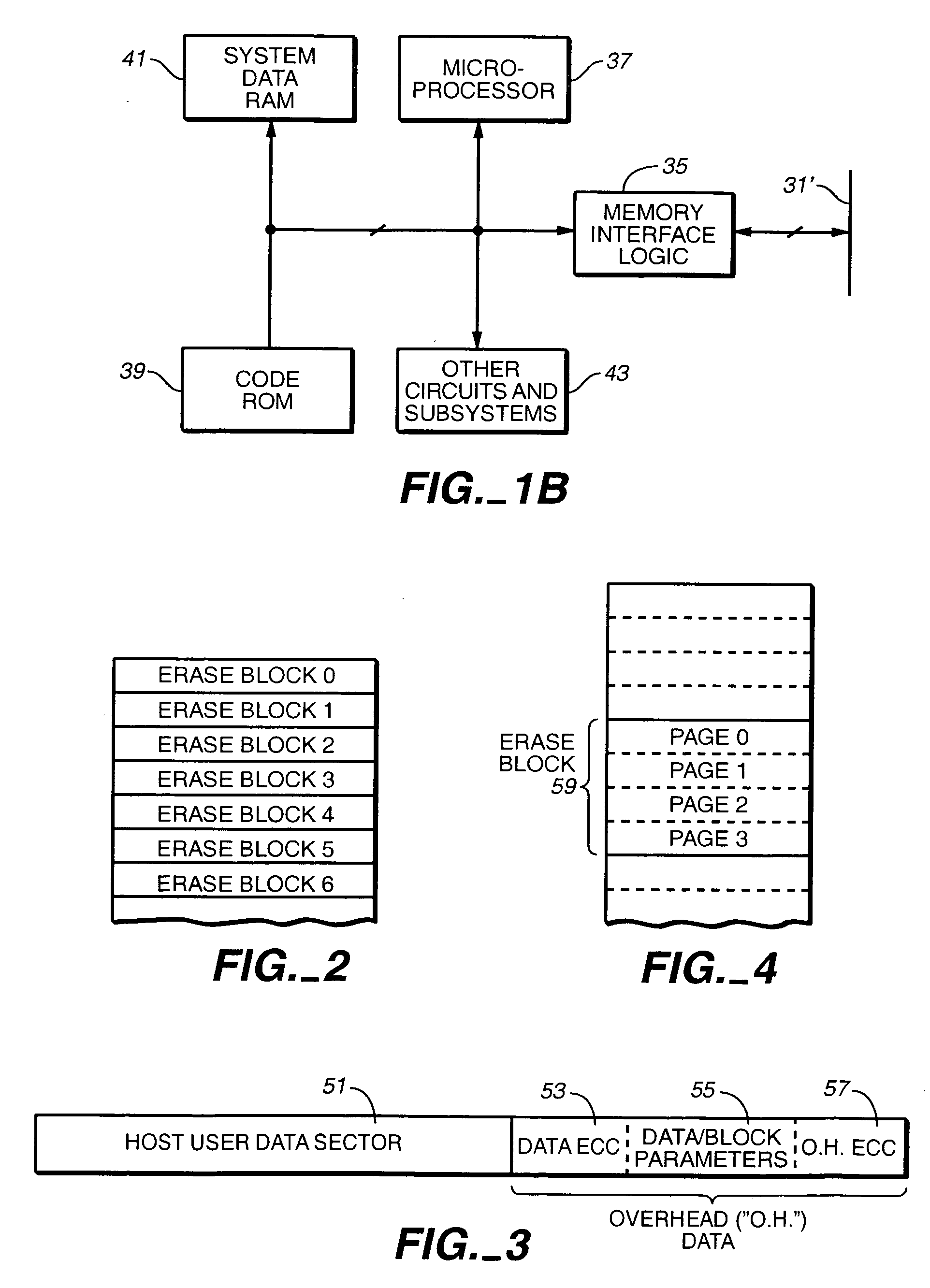
CROSS REFERENCE TO RELATED APPLICATIONS [0001] This application is a continuation-in-part of U.S. patent application Ser. No. 11 / 016,285, filed on Dec. 16, 2004.BACKGROUND OF THE INVENTION [0002] This invention relates generally to the operation of non-volatile flash memory systems, and, more specifically, to more efficient methods of programming data within a non-volatile flash memory. [0003] There are many commercially successful non-volatile memory products being used today, particularly in the form of small form factor cards, which employ an array of flash EEPROM (Electrically Erasable and Programmable Read Only Memory) cells formed on one or more integrated circuit chips. A memory controller, usually but not necessarily on a separate integrated circuit chip, interfaces with a host to which the card is removably connected and controls operation of the memory array within the card. Such a controller typically includes a microprocessor, some non-volatile read-only-memory (ROM), a ...

Claims


Application Information

Patent Timeline
IPC IPC(8): G06F12/00
CPCG06F3/0616G06F3/064G06F3/0679G06F12/0246G06F2212/7203G11C16/102G11C16/34G11C16/10
Inventor SMITH, PETER JOHNGOROBETS, SERGEY ANATOLIEVICHBENNETT, ALAN DAVID
Owner SANDISK TECH LLC
Learn More