Semiconductor device and manufacture method thereof

a semiconductor and semiconductor technology, applied in the direction of printed circuit non-printed electric components association, electrical apparatus construction details, printed electric components, etc., can solve the problems of difficulty in setting up a test jig, small distance between output terminals of mcp, cost disadvantag

Active Publication Date: 2007-09-20
MICRON TECH INC
View PDF17 Cites 23 Cited by
  • Summary
  • Abstract
  • Description
  • Claims
  • Application Information

AI Technical Summary

Problems solved by technology

However, the MCP has a disadvantage in terms of cost since if one or more semiconductor elements in the MCP are defective, the other non-defective semiconductor elements are also treated as defectives.
However, the distance between output terminals thereof is very small.
This causes problems such as difficulty to set up a test jig, and possible cracks if silicon is used alone.
However, since the sphericity of the solder balls is determined by the physical properties of the solder itself, it is impossible to intentionally form the solder balls into a shape elongated in a height direction.
Therefore, the increase of the number of the connection termi

Method used


Image

  • Semiconductor device and manufacture method thereof
  • Semiconductor device and manufacture method thereof
  • Semiconductor device and manufacture method thereof

Examples


Embodiment Construction

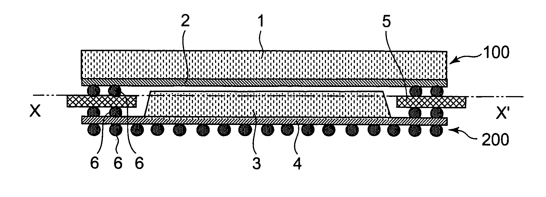
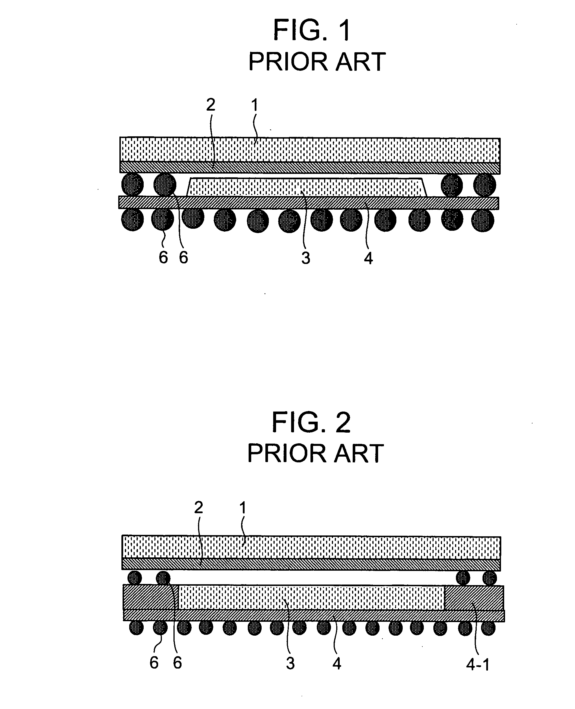
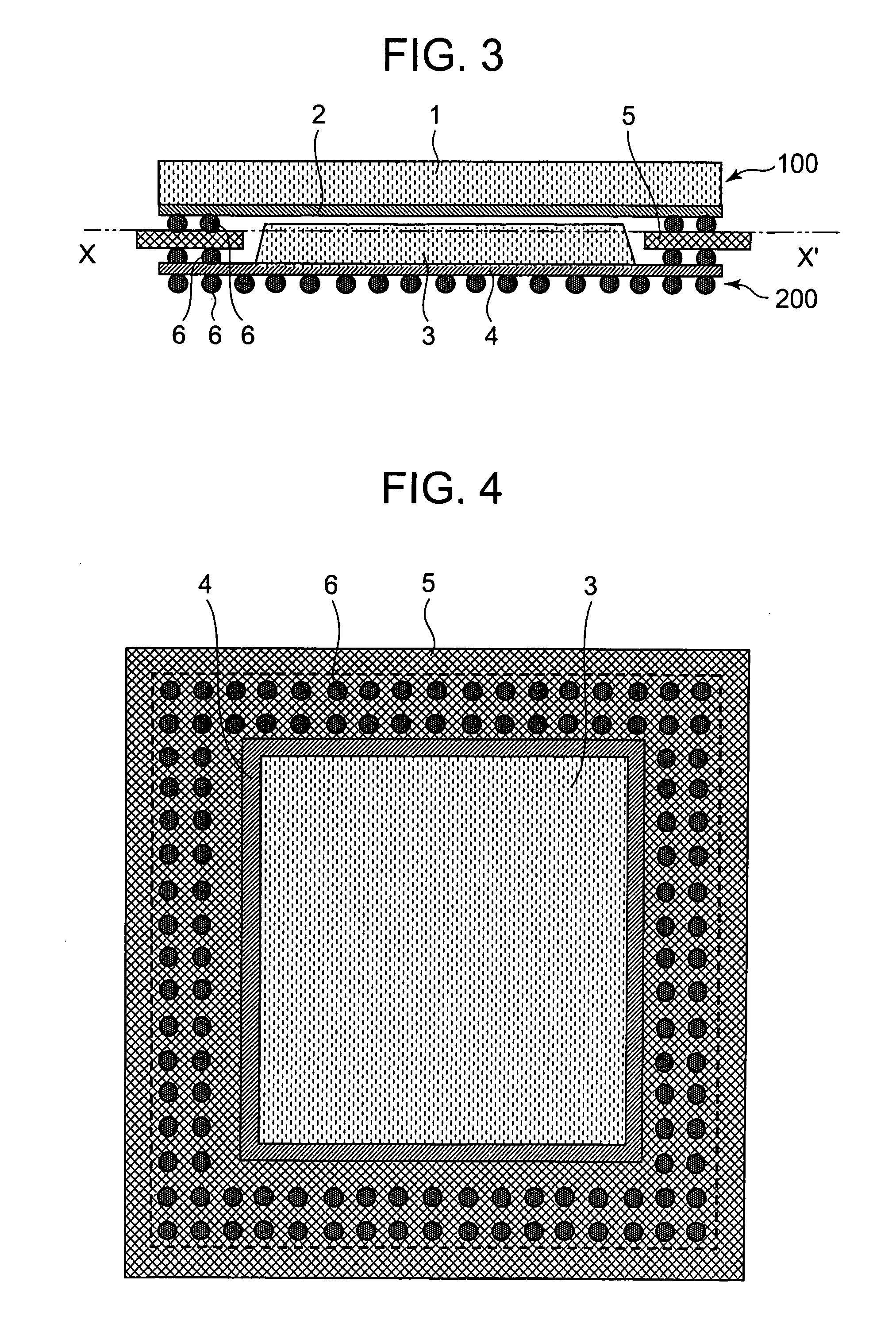
[0040]Description will be made of a semiconductor device and a manufacture method thereof according to the present invention, with reference to FIGS. 3 to 12. FIG. 3 is a side view of a PoP structure according to the present invention. FIG. 4 is a cross-sectional view taken along the X-X′ in FIG. 1, and FIG. 5 is a side view of the PoP structure of FIG. 1 having underfill injected thereinto. FIG. 6 is a side view of a lower package of the PoP structure, and FIG. 7 is a side view of an upper package. FIG. 8 is a top plan view of a joint board frame, and FIG. 9 is a rear plan view of the joint board frame. FIG. 10 is a flowchart illustrating a manufacturing process of the present invention. FIGS. 11A to 11C and FIGS. 12A to 12C are side views showing respective principal steps of the manufacturing process.

[0041]The following description of a semiconductor device according to the present invention will be made on the assumption that upper and lower packages are BGA (Ball Grid Array) pa...


PUM


Abstract

A joint board is arranged between an upper package and a lower package. The arrangement of the joint board makes it possible to reduce the size of solder balls and to arrange them with narrower pitch. The joint board has slightly greater dimensions those of the upper package and the lower package. This makes it possible to prevent underfill from leaking and spreading.

Description

[0001]This application claims priority to prior Japanese patent application JP2006-71130, the disclosure of which is incorporated herein by reference.BACKGROUND OF THE INVENTION[0002]The present invention relates to a semiconductor device, and in particular to a semiconductor device having a PoP (Package on Package) structure in which packages each having a semiconductor element mounted thereon are stacked. The present invention also relates to a manufacture method of such semiconductor device.[0003]In recent years, the package has been reduced in size in order to reduce the size of semiconductor devices following the increase of the operation speed and capacity of the semiconductor devices. Particularly, in case of a portable equipment, use has been made of an MCP (Multi Chip Package) having a plurality of semiconductor elements mounted in the package. However, the MCP has a disadvantage in terms of cost since if one or more semiconductor elements in the MCP are defective, the othe...

Claims


Application Information

Patent Timeline
IPC IPC(8): H05K1/16
CPCH01L23/3128H01L2225/1082H01L2924/15311H01L2924/15331H05K1/141H05K1/182H05K3/0052H05K3/284H05K2201/10515H05K2201/10545H05K2201/10734H01L2924/3511H01L2225/107H01L2225/1023H01L2225/1058H01L2924/15321H01L2224/45144H01L25/105H01L2224/48227H01L21/563H01L24/97H01L25/50H01L2224/16225H01L2924/00
Inventor SHIBAMOTO, MASANORI
Owner MICRON TECH INC
Why Eureka
Try Eureka