

Light emitting material, light emitting element, light emitting device and electronic device
a technology of light emitting elements and light emitting materials, applied in the field of light emitting materials, can solve the problems of large electric power consumption and difficulty in applying it to small and medium-sized displays, and achieve the effect of low cost and reduced power consumption
- Summary
- Abstract
- Description
- Claims
- Application Information
AI Technical Summary
Benefits of technology
Problems solved by technology
Method used
Image

Examples
embodiment mode 1
[0035] Embodiment Mode 1 will describe a light emitting material according to the present invention. The light emitting material of the present invention includes a base material, a luminescent material with a donor-acceptor recombination-type luminescent center, manganese (Mn), and either gallium phosphide (GaP) or gallium antimonide (GaSb).
[0036] As the base material used for the light emitting material, a sulfide, an oxide, or a nitride can be used. As a sulfide, for example, zinc sulfide (ZnS), cadmium sulfide (CdS), calcium sulfide (CaS), yttrium sulfide (Y2S3), gallium sulfide (Ga2S3), strontium sulfide (SrS), barium sulfide (BaS), or the like can be used. As an oxide, for example, zinc oxide (ZnO), yttrium oxide (Y2O3), or the like can be used. Further, as a nitride, for example, aluminum nitride (AIN), gallium nitride (GaN), indium nitride (InN), or the like can be used. Moreover, zinc selenide (ZnSe), zinc telluride (ZnTe), or the like can also be used, and a ternary mixed...
embodiment mode 2
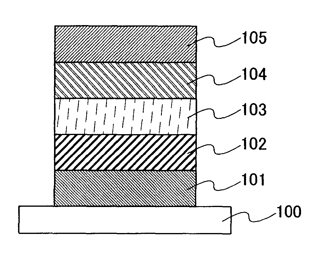
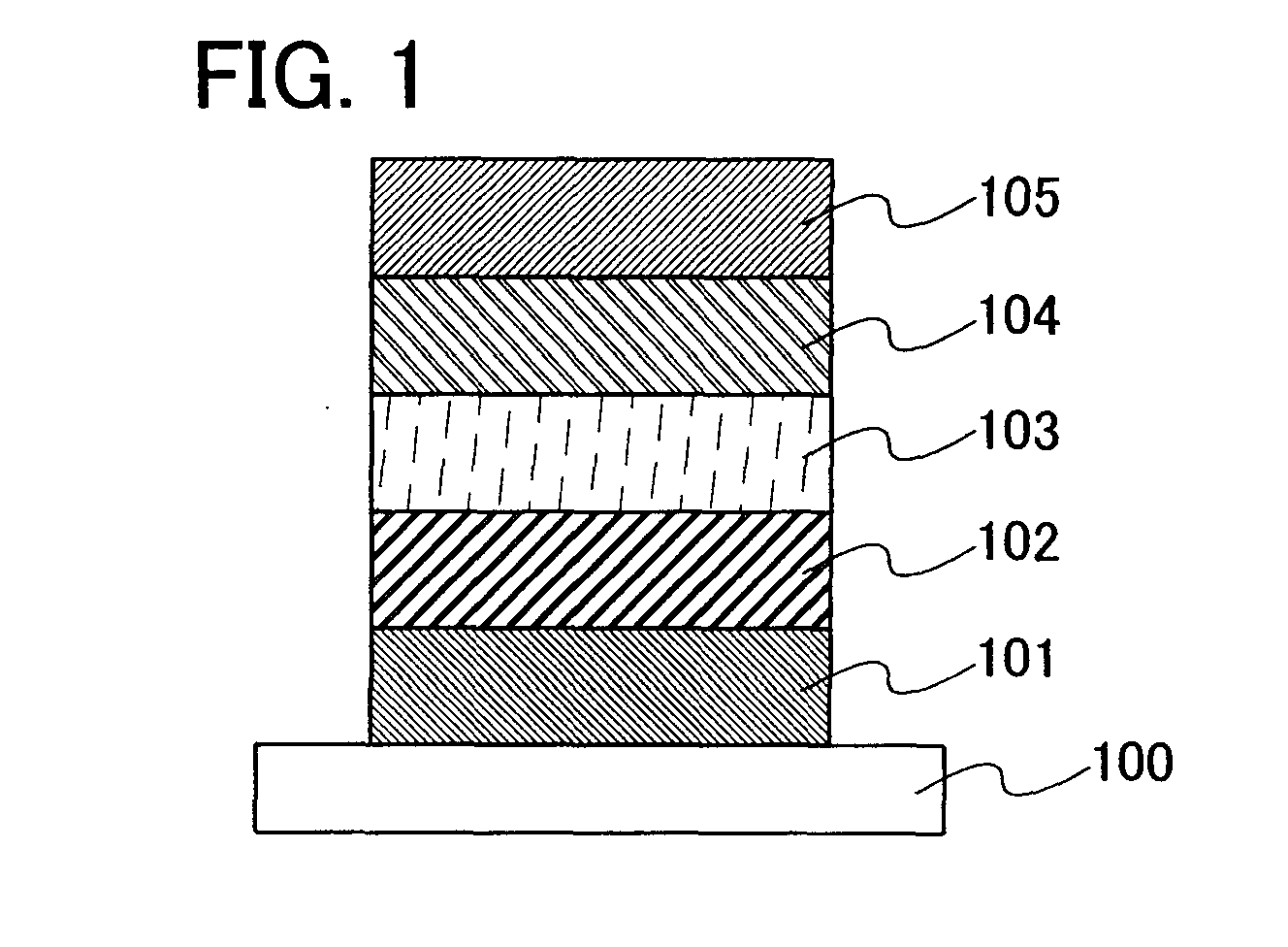
[0048] Embodiment Mode 2 will describe a thin-film type light emitting element according to the present invention with reference to FIG. 1.
[0049] The light emitting element described in this embodiment mode has an element structure including, over a substrate 100, a first electrode 101 and a second electrode 105, a first insulating layer 102 and a second insulating layer 104 in contact with the electrodes, and a light emitting layer 103 between the first insulating layer 102 and the second insulating layer 104. The light emitting element described in this embodiment mode emits light from the light emitting layer 103 by voltage application between the first electrode 101 and the second electrode 105 and can be operated by either DC drive or AC drive.
[0050] The substrate 100 is used as a support of the light emitting element. For the substrate 100, glass, plastic, or the like can be used, for example. Note that another material may be used as long as it functions as a support during...
embodiment mode 3
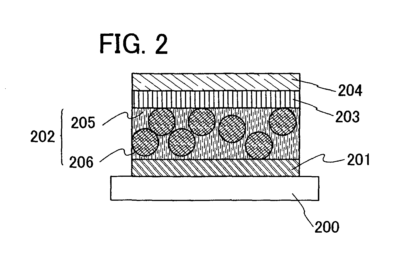
[0056] Embodiment Mode 3 will describe a dispersion type light emitting element according to the present invention with reference to FIG. 2.
[0057] The light emitting element shown in this embodiment mode has an element structure in which a first electrode 201, a second electrode 204, an insulating layer 203 in contact with the second electrode, and a light emitting layer 202 between the first electrode 201 and the insulating layer 203 are provided over a substrate 200. The light emitting element described in this embodiment mode emits light from the light emitting layer 202 by voltage application between the first electrode 201 and the second electrode 204 and can be operated by either DC drive or AC drive.
[0058] The light emitting layer 202 is a film in which particles of the light emitting material 205 are dispersed in a binder 206. The binder is a substance used for fixing the particles of the light emitting material in a dispersed state and for keeping a shape as a light emitt...
PUM
 Abstract
Description
Claims
Application Information