
Semiconductor device and manufacturing method of the same

a semiconductor and semiconductor technology, applied in semiconductor devices, transistors, electrical devices, etc., can solve the problems of semiconductor substrate warping, difficulty in thinning semiconductor substrates, and increasing costs,

Inactive Publication Date: 2007-09-20
SANYO ELECTRIC CO LTD +1
View PDF10 Cites 54 Cited by
  • Summary
  • Abstract
  • Description
  • Claims
  • Application Information

AI Technical Summary

Problems solved by technology

However, there are technological problems and difficulties in thinning the semiconductor substrate.
However, the above-described method requires the supporting substrate itself, processes of attaching and removing the supporting substrate, or the like, thereby increasing the cost.
Furthermore, the strength of the semiconductor substrate 301 in the completed device is still low, so that a difference in coefficient of thermal expansion between the collector electrode and the semiconductor substrate easily causes the semiconductor substrate to warp.

Method used


Image

  • Semiconductor device and manufacturing method of the same
  • Semiconductor device and manufacturing method of the same
  • Semiconductor device and manufacturing method of the same

Examples


Embodiment Construction

[0042] A semiconductor device and a method of manufacturing the semiconductor device of the invention will be described in detail referring to figures.

[0043] First, a case where the invention is applied to a vertical MOS transistor will be described in detail referring to FIGS. 1 to 15.

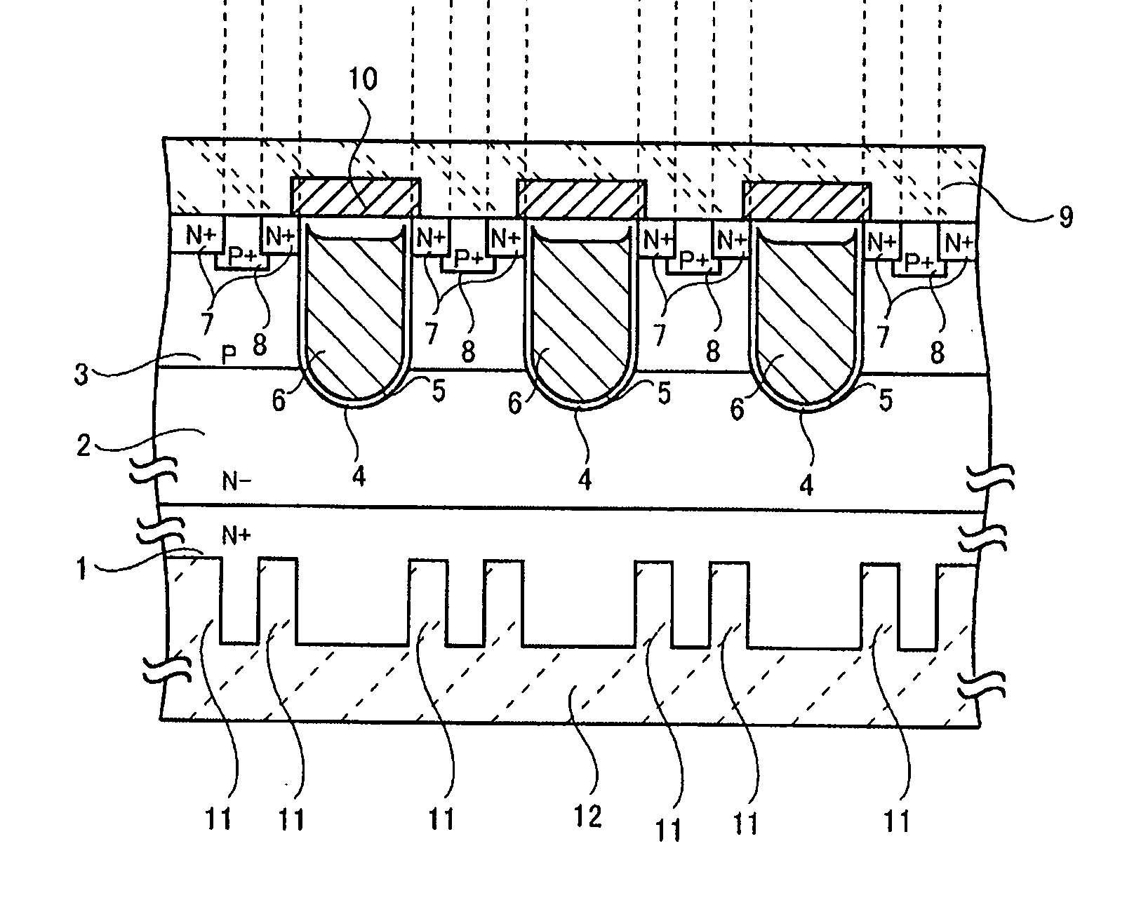
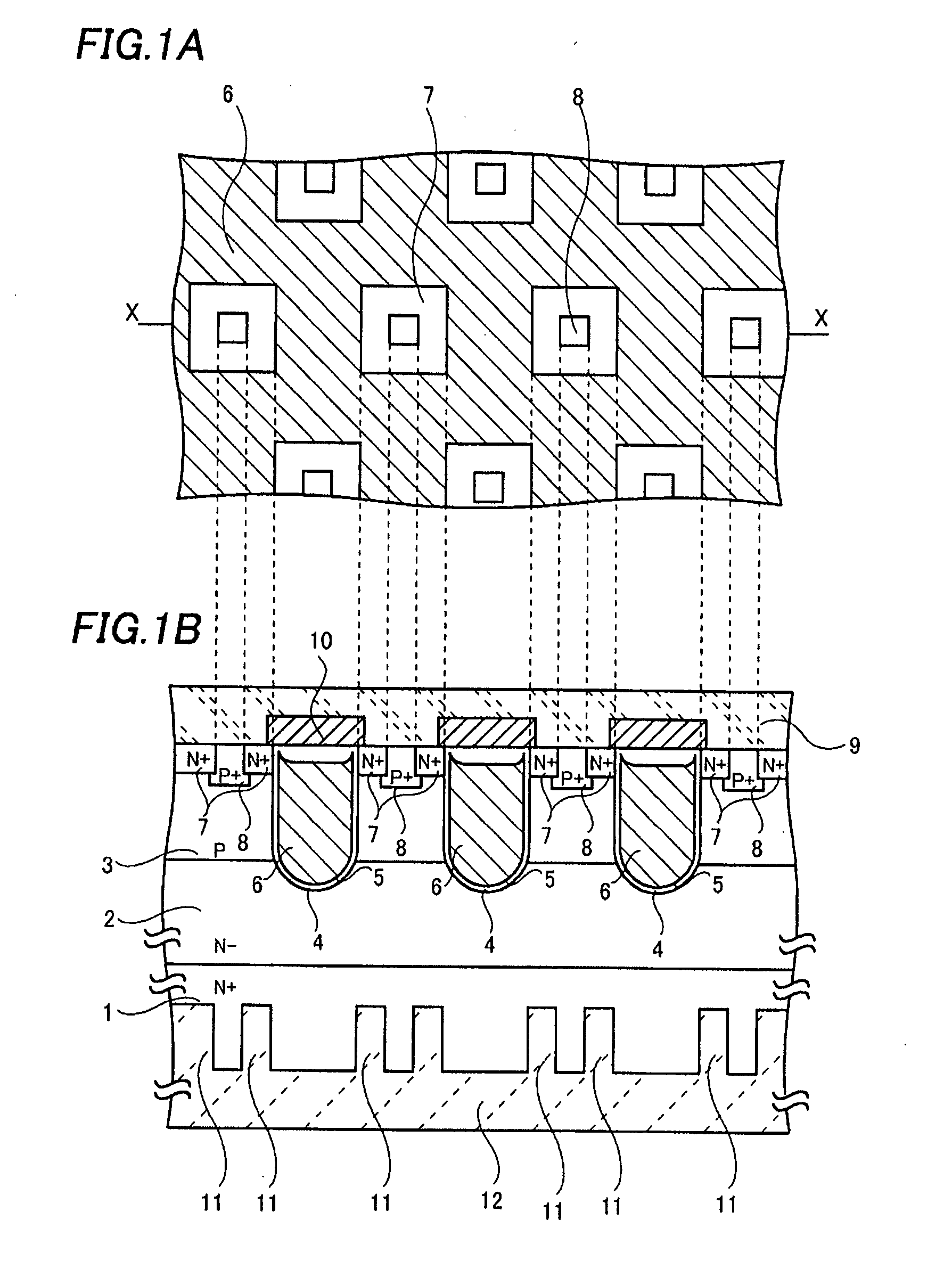
[0044]FIGS. 1A and 1B show the vertical MOS transistor of the invention. FIG. 1A is its plan view and FIG. 1B is a cross-sectional view along line X-X of FIG. 1A.

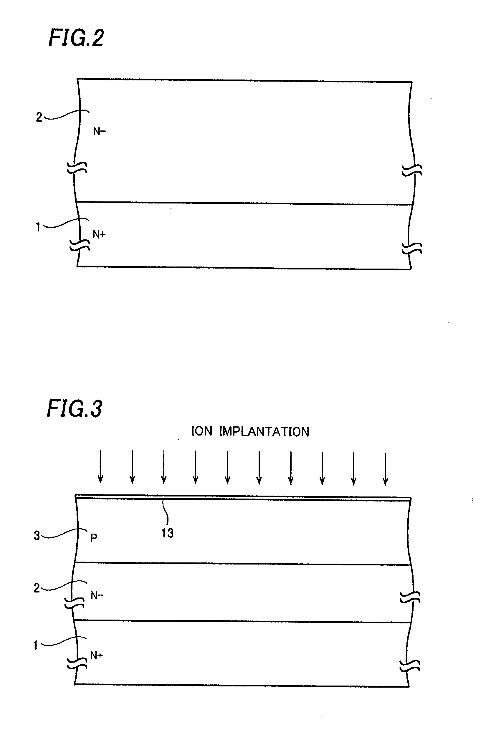
[0045] An N−-type epitaxial layer 2 is formed on an N-type semiconductor substrate 1, and a P-type channel layer 3 is formed on its front surface.

[0046] Trench grooves 4 are formed from the front surface of the channel layer 3 to the epitaxial layer 2. Conductive layers made of polysilicon films are embedded in the trench grooves 4 to form gate electrodes 6, being surrounded by insulation layers 5.

[0047] N+-type source layers 7 are formed on the front surface of the epitaxial layer 2, being adjacent to the trench grooves 4, and P+-type b...


PUM


Abstract

Thinning a semiconductor substrate has been needed for reducing on-resistance in a semiconductor device such as a vertical MOS transistor, IGBT, or the like where a high current flows in the semiconductor substrate in a vertical direction. In this case, the thinning is performed to the extent that the semiconductor substrate does not warp with a heat treatment, so that there is a limitation in reduction of on-resistance. In the invention, openings such as trench holes are formed on a back surface side of a semiconductor substrate. Then, a drain electrode is formed being electrically connected with bottoms of these openings. In this case, a current path is formed short corresponding to the depths of the openings, thereby easily achieving low on-resistance.

Description

CROSS-REFERENCE OF THE INVENTION [0001] This invention claims priority from Japanese Patent Application Nos. 2006-072645, 2006-215906 and 2007-042703, the contents of which are incorporated herein by reference in their entirety. BACKGROUND OF THE INVENTION [0002] 1. Field of the Invention [0003] The invention relates to a semiconductor device and a method of manufacturing the same, particularly to a semiconductor device where a high current flows in a vertical direction of a semiconductor substrate and a method of manufacturing the same. [0004] 2. Description of the Related Art [0005] The vertical MOSFET is suitable as a high current element since it possesses a larger area through which a current flows than the lateral MOSFET where a source electrode and a drain electrode are arranged on the same surface. [0006]FIG. 27 is a conventional cross-sectional view of an example of the vertical MOS transistor. [0007] An N−-type epitaxial layer 202 is formed on an N+-type semiconductor subs...

Claims


Application Information

Patent Timeline
Patent Type & Authority Applications(United States)
IPC IPC(8): H01L29/94
CPCH01L29/0653H01L2924/10158H01L29/0696H01L29/0834H01L29/0886H01L29/41716H01L29/41741H01L29/41766H01L29/66734H01L29/7395H01L29/7397H01L29/7398H01L29/7802H01L29/7809H01L29/7813H01L29/0657H01L29/73
Inventor YANAGIDA, MASAMICHIKAMEYAMA, KOUJIROOKADA, KIKUO
Owner SANYO ELECTRIC CO LTD
Features
  • Generate Ideas
  • Intellectual Property
  • Life Sciences
  • Materials
  • Tech Scout
  • Unparalleled Data Quality
  • Higher Quality Content
  • 60% Fewer Hallucinations
Learn More