Semiconductor device including MOS transistor having LOCOS offset structure and manufacturing method thereof

a technology of mos transistor and semiconductor device, which is applied in the direction of semiconductor device, semiconductor/solid-state device details, electrical apparatus, etc., can solve the problem of not disclosed manufacturing method for manufacturing high-voltage locos

Inactive Publication Date: 2007-09-20
RICOH KK
View PDF3 Cites 16 Cited by
  • Summary
  • Abstract
  • Description
  • Claims
  • Application Information

AI Technical Summary

Benefits of technology

[0039] Other objects, features and advantage of the present invention will become more apparent from the following detailed description when read in conjunction with the accompanying drawings.

Problems solved by technology

However, there has been no disclosed manufacturing method for manufacturing a high-voltage LOCOS offset transistor configured to eliminate the off-leakage current without the P−region (LDD (Lightly Doped Drain)) and a normal low-voltage transistor configured to eliminate the off-leakage current with the P−region on the same semiconductor substrate.

Method used


Image

  • Semiconductor device including MOS transistor having LOCOS offset structure and manufacturing method thereof
  • Semiconductor device including MOS transistor having LOCOS offset structure and manufacturing method thereof
  • Semiconductor device including MOS transistor having LOCOS offset structure and manufacturing method thereof

Examples


Embodiment Construction

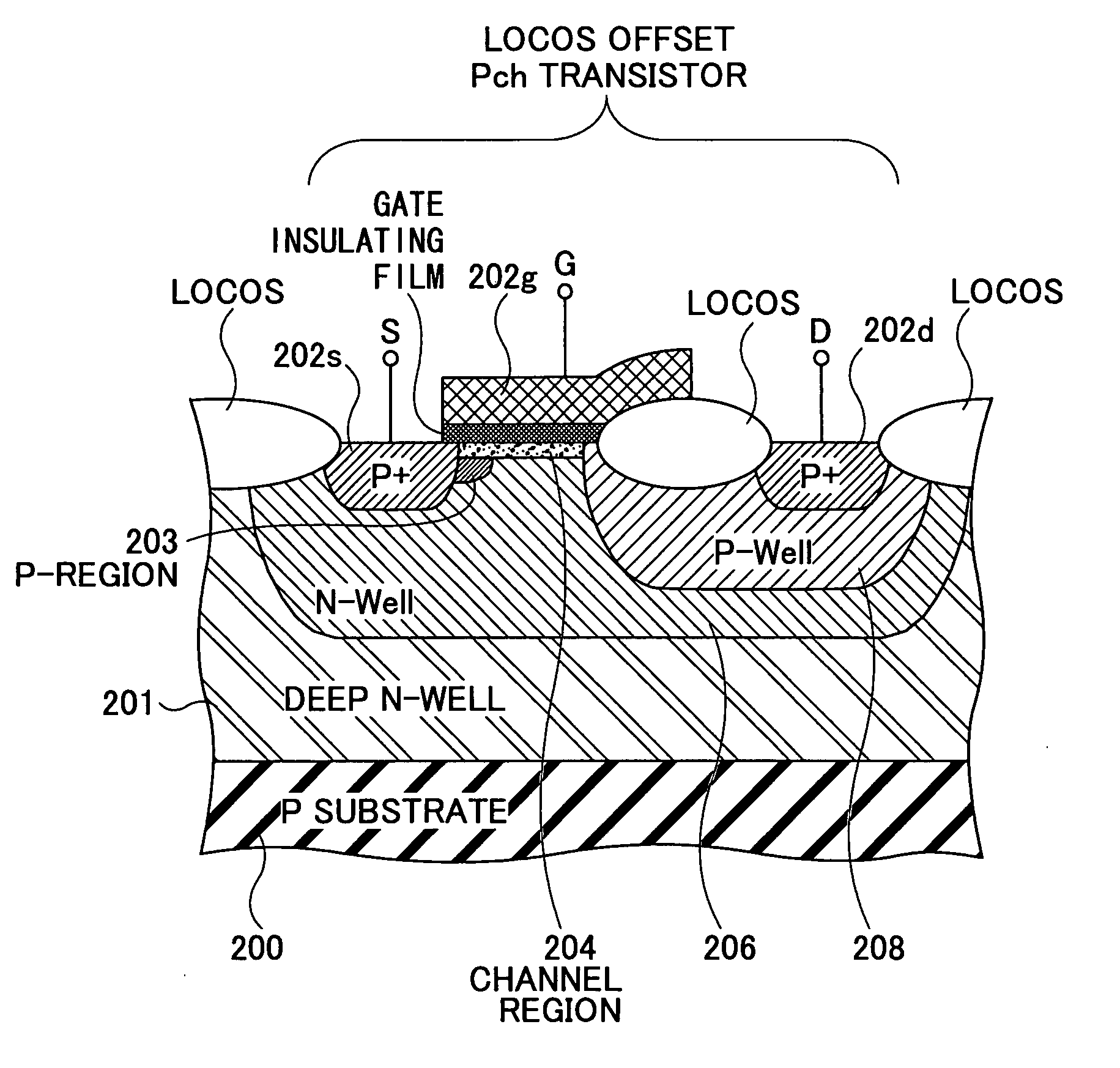
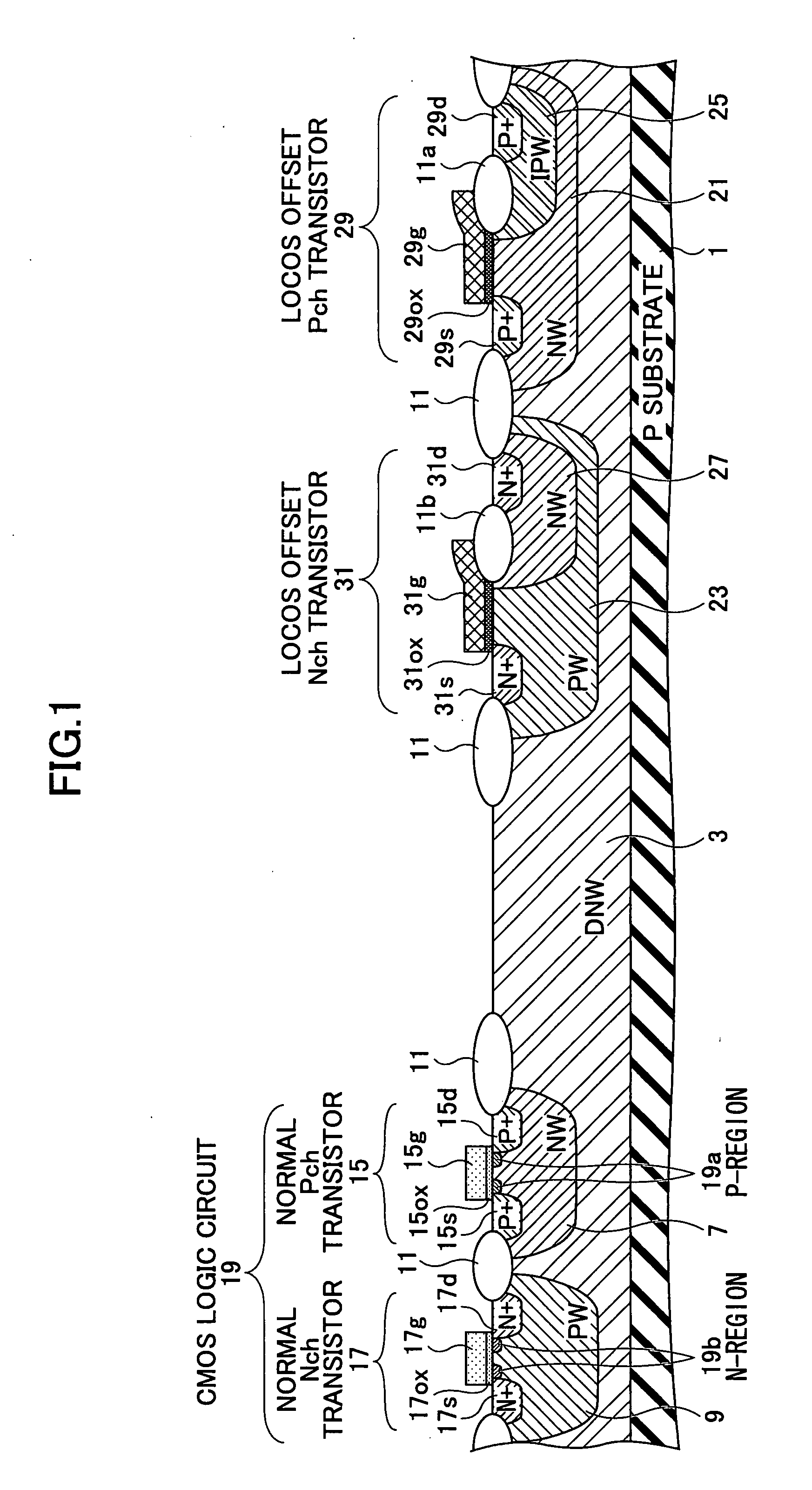
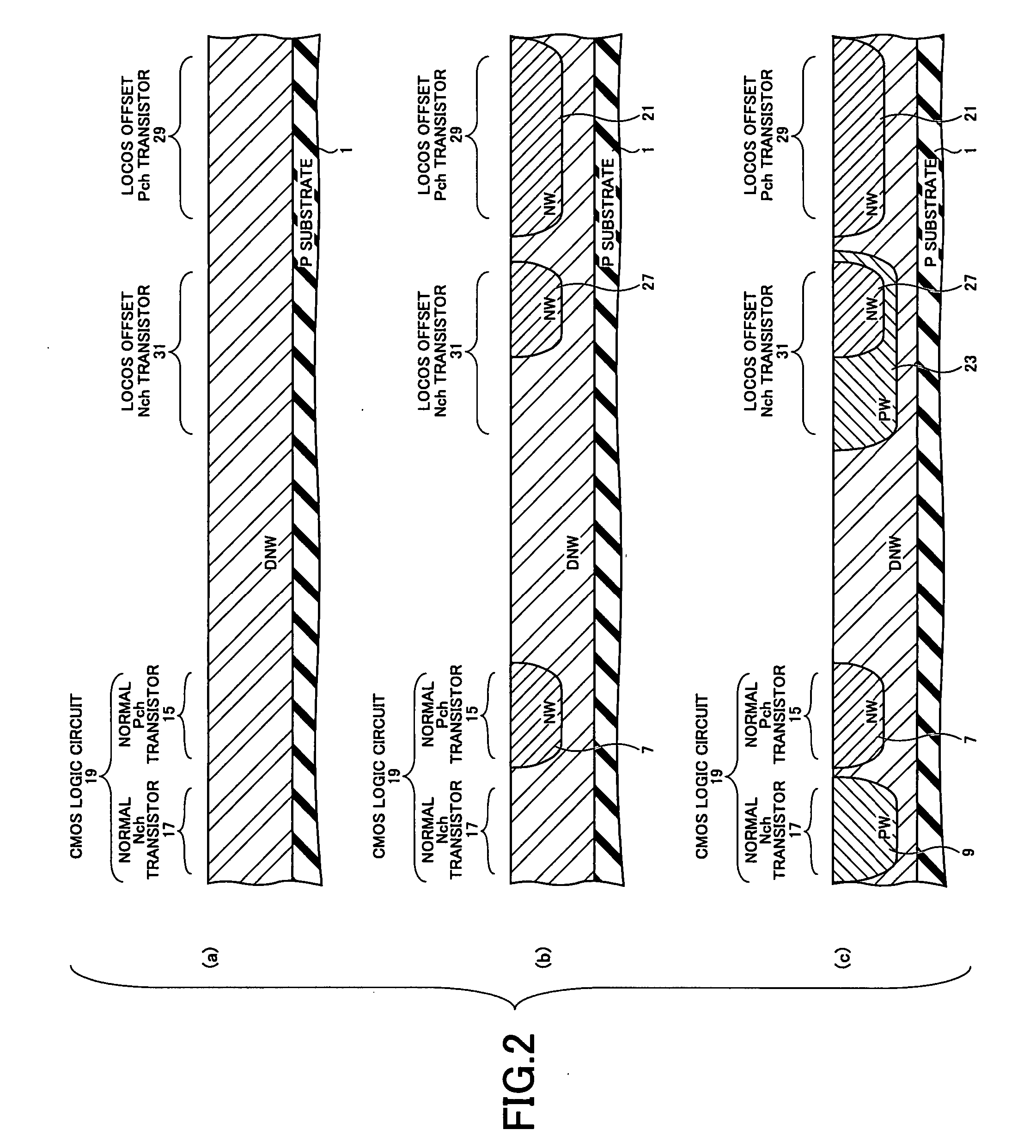
[0050]FIG. 1 is a cross-sectional view showing an example of a semiconductor device manufactured in a method for manufacturing a semiconductor device according to the present invention. In the present invention, at least one Nch or Pch LOCOS offset transistor and at least one normal Nch or Pch transistor are manufactured on the same semiconductor substrate. In the present embodiment, four types of transistors, namely, a LOCOS offset Nch transistor, a LOCOS offset Pch transistor, a normal Pch transistor, and a normal Nch transistor are manufactured on the same semiconductor substrate as an example. However, it is possible to apply the present invention to any combination as long as at least one LOCOS offset transistor and at least one normal transistor are used. It is possible to form a CMOS transistor using a normal Nch transistor and a normal Pch transistor.

[0051] A deep N-well (DNW) 3 is formed on a P substrate 1. On the P substrate 1, a normal N-well (NW) 7, a normal P-well (PW)...


PUM


Abstract

A disclosed semiconductor device includes: a semiconductor substrate; at least one normal transistor disposed on the semiconductor substrate; and at least one LOCOS offset transistor disposed on the semiconductor substrate. The normal transistor has an LDD region between a channel and a source and between the channel and a drain. And the LOCOS offset transistor has no LDD region between a channel and a source and between the channel and a drain.

Description

BACKGROUND OF THE INVENTION [0001] 1. Field of the Invention [0002] The present invention generally relates to a technique for manufacturing a high-voltage MOS transistor having a LOCOS (LOCal Oxidation of Silicon) offset structure and a normal low-voltage transistor on the same semiconductor substrate and more particularly to a technique for manufacturing a high-voltage MOS transistor having the LOCOS structure capable of reducing an off-leakage current even when a source and a drain are reversed and a normal low-voltage transistor on the same semiconductor substrate. The present invention is especially effective when applied to a transistor constituting a boost DC / DC converter. [0003] 2. Description of the Related Art [0004] In MOS transistor techniques, it is well-known that an off-leakage current in a Pch transistor is reduced when an impurity with low concentration is implanted between a source and a channel or between a drain and the channel and a region (what is called a P−re...

Claims


Application Information

Patent Timeline
Patent Type & Authority Applications(United States)
IPC IPC(8): H01L23/62
CPCH01L21/823412H01L21/823418H01L21/823814H01L21/823892H01L27/088H01L29/7835H01L29/1083H01L29/42368H01L29/6659H01L29/66659H01L29/7833H01L27/0922
Inventor KIJIMA, MASATO
Owner RICOH KK
Why Eureka
Try Eureka