Electrostatic chuck

a technology of electrostatic chuck and chuck body, which is applied in the direction of relays, magnets, vacuum evaporation coatings, etc., can solve the problems of difficult to process each flat substrate w under the same condition, difficult to keep the flat substrate w at a constant temperature, and difficult to keep the top surface uniform, etc., to prevent a large variation in thermal conductivity, and weak electrostatic attraction force

Active Publication Date: 2007-09-20
SUMITOMO OSAKA CEMENT CO LTD +1
View PDF10 Cites 62 Cited by
  • Summary
  • Abstract
  • Description
  • Claims
  • Application Information

AI Technical Summary

Benefits of technology

[0053] According to the above-mentioned structure, in the electrostatic chuck, when the height of the second wall portion from the step portion is smaller than 1 μm, particles are likely to be adhered to the rear surface of a flat substrate, and a large variation in thermal conductivity occurs due to the particles adhered to the rear surface of the flat substrate. Meanwhile, when the...

Problems solved by technology

However, in the electrostatic chuck 1 according to the related art, as the number of flat substrates W processed increases, the top surfaces 4a of the columnar protrusions 4 of the electrostatic chuck body 2 are worn away due to contact with the flat substrate W, and the states of the top surfaces 4a of the columnar protrusions 4 vary over time, which makes it difficult to keep uniform contact between the top surfaces 4a and the flat substrate W.
In this case, thermal conductivity between the electrostatic chuck body 2 and the flat substrate W varies over time, which makes it difficult to keep the flat substrate W at a constant temperature.
A...

Method used


Image

  • Electrostatic chuck
  • Electrostatic chuck
  • Electrostatic chuck

Examples


first embodiment

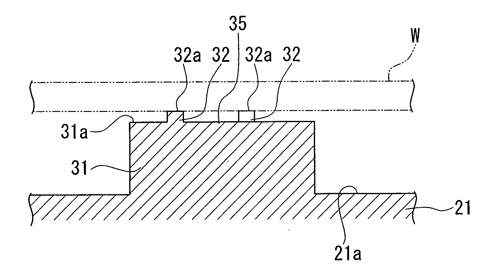
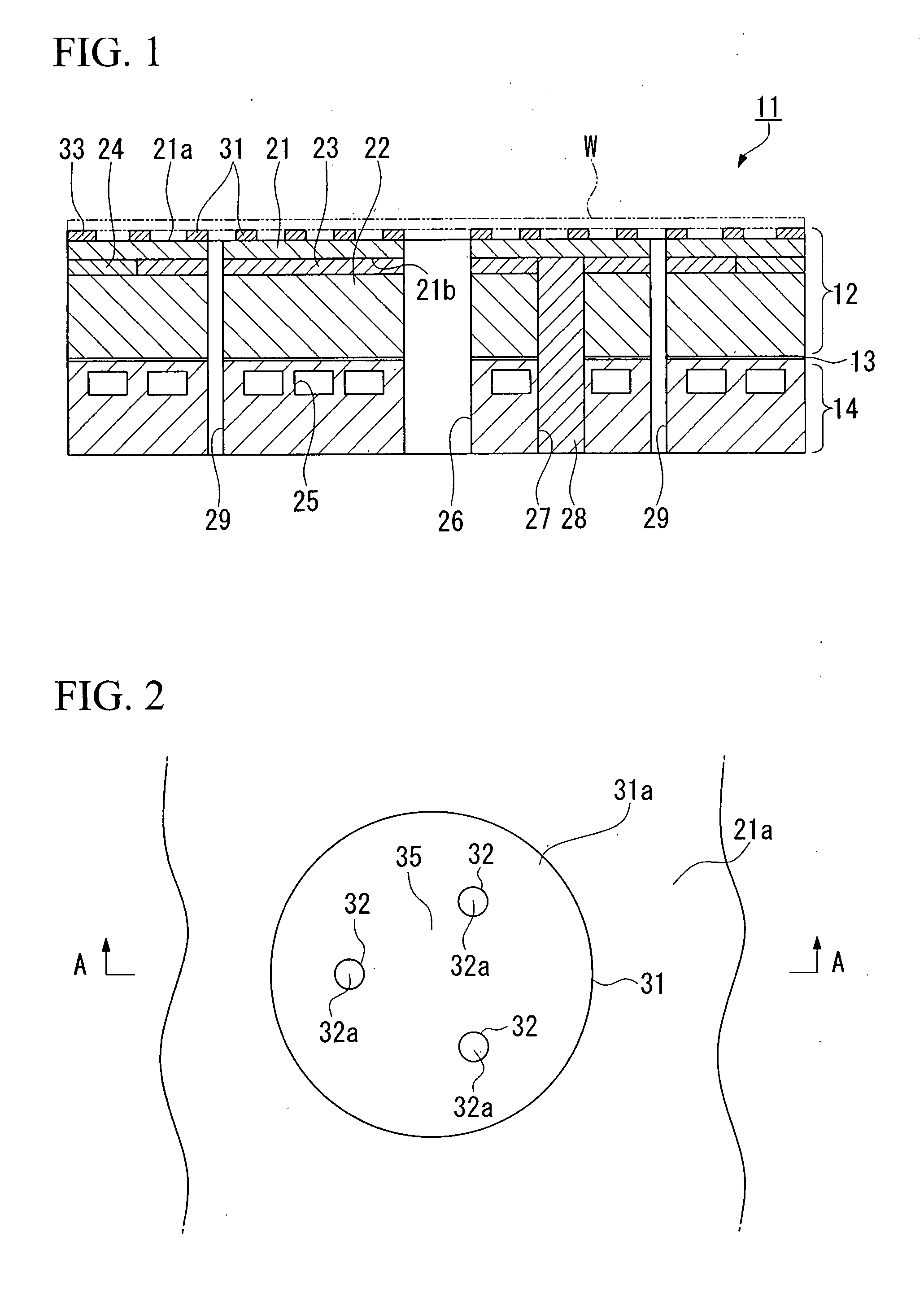
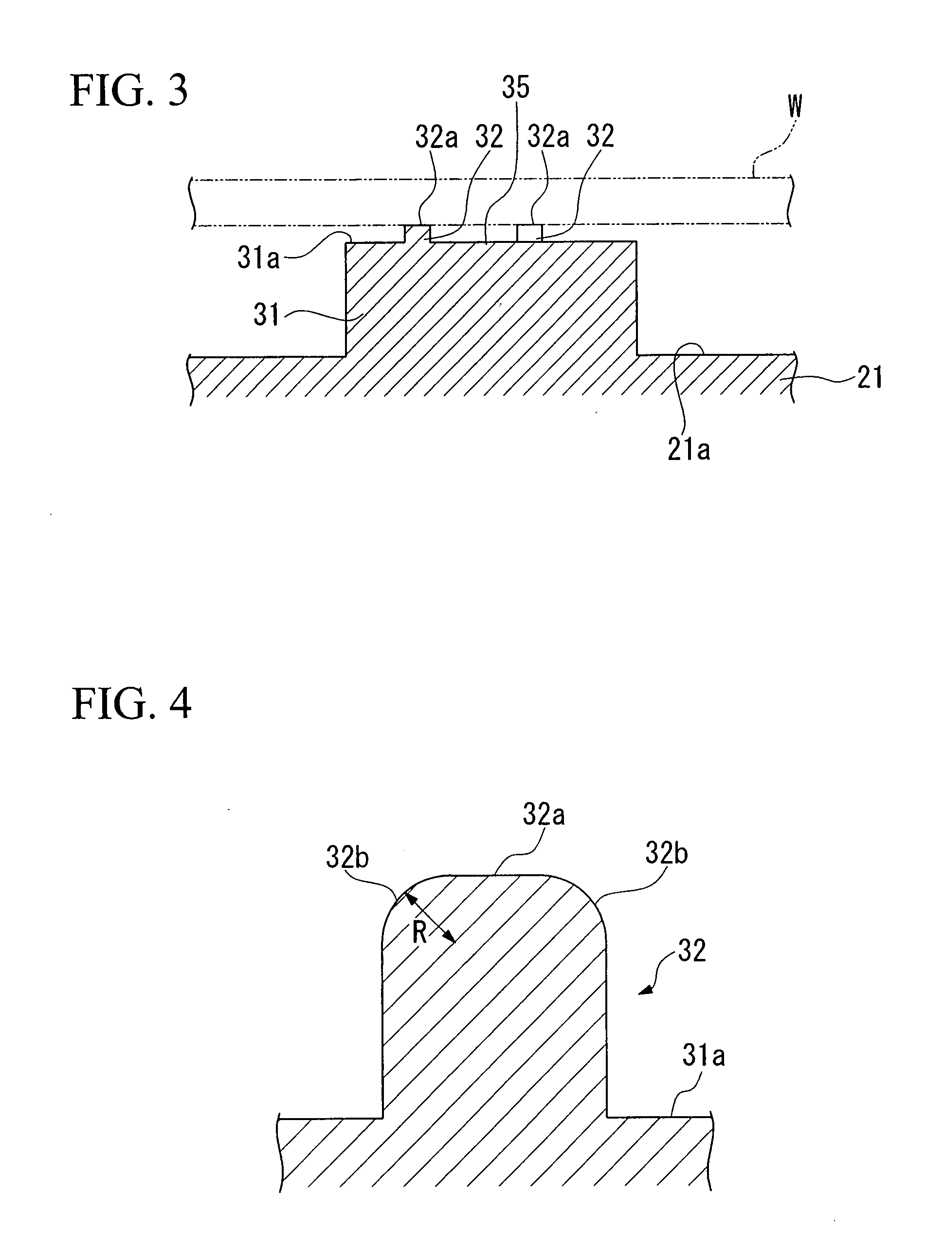
[0069]FIG. 1 is a cross-sectional view illustrating an electrostatic chuck according to a first embodiment of the invention, FIG. 2 is an enlarged plan view illustrating the periphery of a circumferential portion of the electrostatic chuck, and FIG. 3 is a cross-sectional view taken along the line II-II of FIG. 2. An electrostatic chuck 11 includes a disk-shaped body 12 and a temperature adjusting base member 14 that is formed of a metallic material and is bonded to a lower surface of the body 12 by a silicon resin adhesive 13.

[0070] The body 12 includes a dielectric plate 21 that is an upper surface (one surface 21a) serving as a mounting surface on which a test sample W, such as a semiconductor wafer, a metal wafer, or a glass plate, is loaded, a disk-shaped insulating member 22 that is arranged opposite to a lower surface 21b (the other surface) of the dielectric plate 21, an internal electrode 23, and a ring-shaped insulting member 24 that is arranged to surround the internal e...

second embodiment

[0157]FIG. 6 is a plan view illustrating the vicinity of a circumferential portion of an electrostatic chuck according to a second embodiment of the invention, and FIG. 7 is a cross-sectional view taken along the line VII-VII of FIG. 6. An electrostatic chuck 51 according to the second embodiment differs from the electrostatic chuck 11 according to the first embodiment in that a step portion 52 having a rectangular shape in sectional view is formed along the circumference of the wall portion 33 inside a top surface 33a of the wall portion 33, a flat substrate W is loaded on the top surface of a ring-shaped wall portion 33B, and the step portion 52 and the wall portion 33B control the flow of a cooling gas, such as He.

[0158] The width of the wall portion 33B is in the range of 10 μm to 50 μm, and the height thereof is in the range of 1 μm to 10 μm.

[0159] When the width of the wall portion 33B is smaller than 10 μm, the time required to perform a waferless dry-cleaning process is le...

third embodiment

[0161]FIG. 8 is a plan view illustrating the vicinity of a circumferential portion of an electrostatic chuck according to a third embodiment of the invention, and FIG. 9 is a cross-sectional view taken along the line IX-IX of FIG. 8. An electrostatic chuck 61 according to the third embodiment differs from the electrostatic chuck 51 according to the second embodiment in that a plurality of minute projections 32 are provided on the step portion 52, a flat substrate W is loaded on the top surface of a ring-shaped wall portion 33B and the top surfaces 32a of the minute projections 32, and the step portion 52 and the wall portion 33B control the flow of a cooling gas such as He.

[0162] The sectional area of the minute projection 32 is preferably equal to or larger than 8×10⁻⁵ mm2 and equal to or smaller than 2×10⁻³ mm2.

[0163] The electrostatic chuck 61 according to this embodiment can achieve the same effects as the electrostatic chuck 51 according to the second embodiment.

[0164] In pa...


PUM

PropertyMeasurementUnit
Fractionaaaaaaaaaa
Fractionaaaaaaaaaa
Fractionaaaaaaaaaa

Abstract

The invention provides an electrostatic chuck capable of widening a temperature range when the temperature of a flat substrate is controlled and reducing a variation in thermal conductivity between the electrostatic chuck and the flat substrate over time. According to an aspect of the invention, an electrostatic chuck includes: a body that has an internal electrode for attracting a flat substrate by an electrostatic force provided therein; a plurality of protrusions that are formed on one surface of the body, serving as an electrostatic attraction surface; and one or more minute projections that are provided on each of top surfaces of some or all of the plurality of protrusions. In the electrostatic chuck, a region of the top surface of each of the minute projections on which the flat substrate is loaded is referred to as a mounting surface, and the total area of the mounting surfaces of the minute projections is equal to or larger than 0.01% and equal to or smaller than 2% of the area of the electrostatic attraction surface.

Description

[0001] This application claims priority to and the benefit of Japanese Patent Application No. 2006-022381, filed on Jan. 31, 2006, and U.S. Provisional Patent Application No. 60 / 775,892, filed on Feb. 23, 2006, the entire contents of which are hereby incorporated by reference as if fully set forth herein.BACKGROUND OF THE INVENTION [0002] 1. Field of the Invention [0003] The present invention relates to an electrostatic chuck used to fix a flat substrate (flat test sample), such as a semiconductor wafer, a metal wafer, or a glass plate, that is used to manufacture a liquid crystal display (LCD) and semiconductor devices, such as IC, LSI, and VLSI. [0004] 2. Description of Related Art [0005] In the related art, in a method of manufacturing a semiconductor device or a liquid crystal display device, various processes are performed on the surface of a flat substrate, such as a semiconductor wafer, a metal wafer, or a glass plate. During these processes, in order to fix the flat substrat...

Claims


Application Information

Patent Timeline
IPC IPC(8): H01H47/00
CPCC23C14/505C23C16/4581H01L21/6875H01L21/6831C23C16/4586
Inventor SASAKI, YASUHARUUEDA, TAKEHIRONAKAGAWA, YUSUKENAGAYAMA, NOBUYUKIOKAJO, TAKETOSHIKOSAKAI, MAMORU
Owner SUMITOMO OSAKA CEMENT CO LTD
Why Eureka
Try Eureka