Semiconductor integrated circuit device and related method

Active Publication Date: 2007-09-27
SAMSUNG ELECTRONICS CO LTD
View PDF12 Cites 32 Cited by
  • Summary
  • Abstract
  • Description
  • Claims
  • Application Information

AI Technical Summary

Benefits of technology

[0007]Embodiments of the invention provide a semiconductor integrated circuit device having reduced contact resistance and an improved electrical characteristic(s), and a method for fabricating t

Problems solved by technology

Thus, contacts disposed in a cell array region of a semiconductor substrate and contacts disposed in a peripheral circuit region of a semiconductor substrate cannot be formed using a single process.
In addition, as the design rule for semiconductor integrated circuit devices has been reduced, problems have arisen in the peripheral circuit region as well as the cell array region.
Examples of such problems are difficulty acquiring the open mar

Method used


Image

  • Semiconductor integrated circuit device and related method
  • Semiconductor integrated circuit device and related method
  • Semiconductor integrated circuit device and related method

Examples


Example

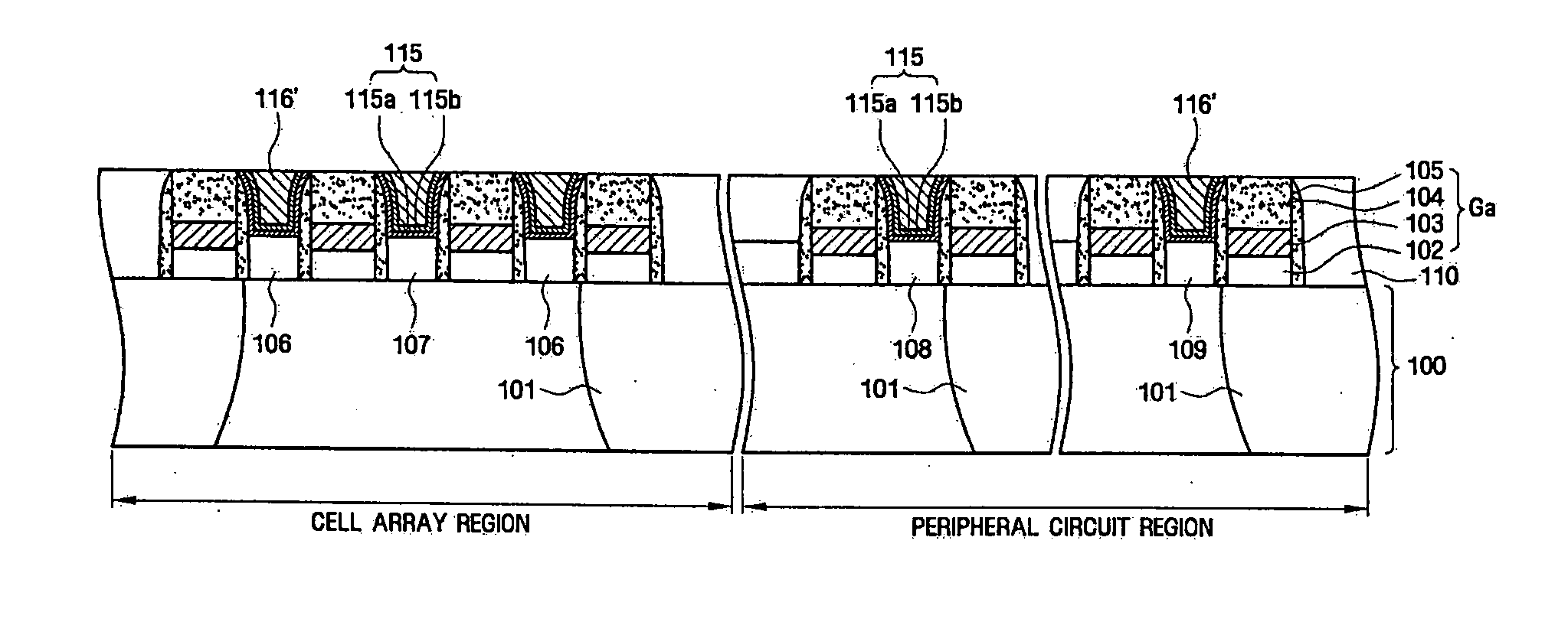
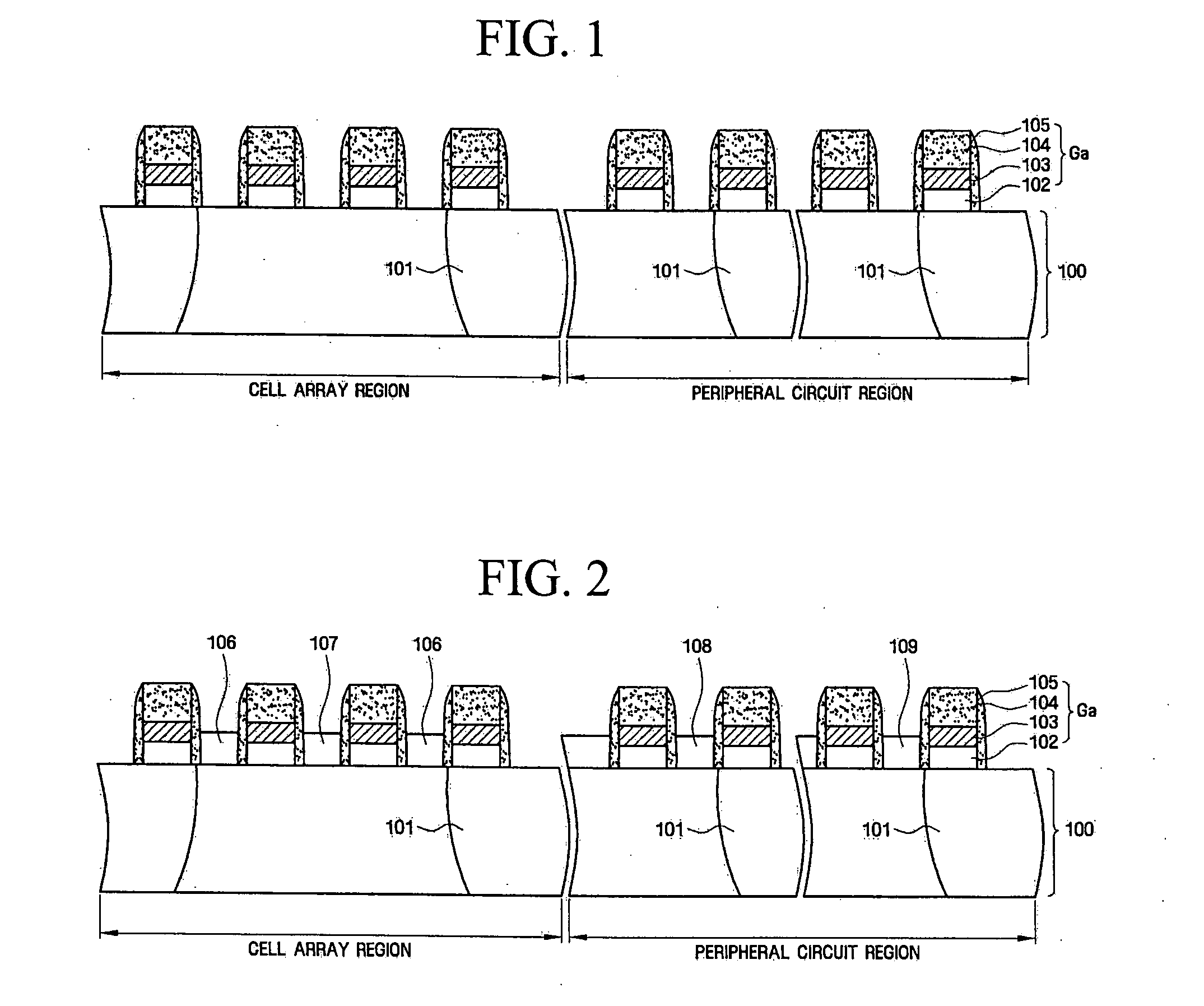
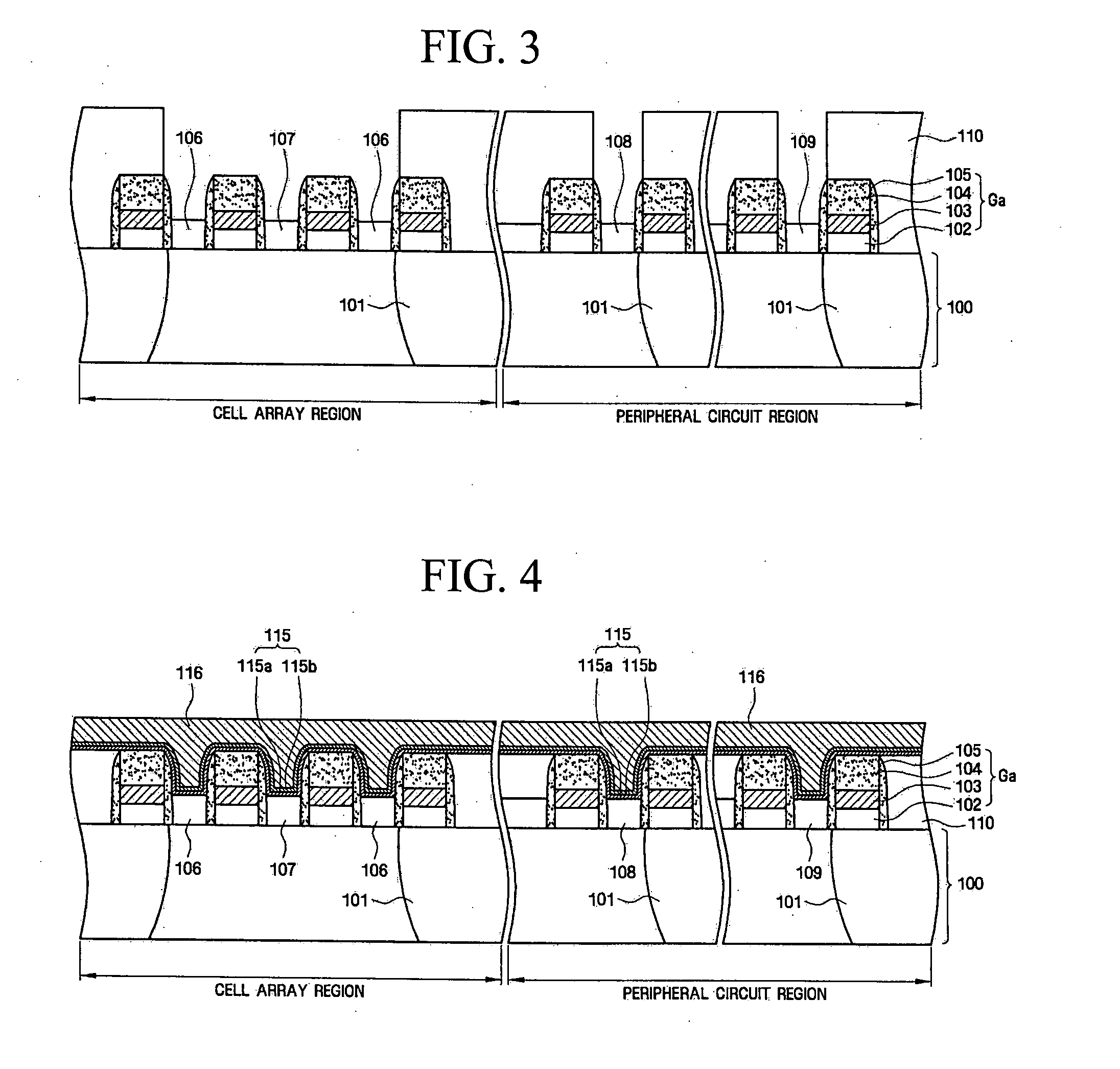
[0014]As used herein, when a first element or layer is described as being “on,”“connected to,” or “coupled to” a second element or layer, the first element or layer may be directly on, directly connected to, or directly coupled to the second element or layer, or intervening elements and / or layers may be present. In contrast, when a first element or layer is described as being “directly on,”“directly connected to,” or “directly coupled to” a second element or layer, no intervening elements and / or layers are present. As used herein, the term “and / or” may indicate any combination of one or more of the listed items.

[0015]The illustrated embodiments of the invention will be described below with reference to drawings showing exemplary cross-sections of the illustrated embodiments. In practice, the actual shapes of elements illustrated in the drawings may deviate from the shapes shown in the drawings in accordance with manufacturing techniques and / or tolerances. Accordingly, the illustrate...


PUM


Abstract

Embodiments of the invention provide a semiconductor integrated circuit device and a method for fabricating the device. In one embodiment, the method comprises forming a plurality of preliminary gate electrode structures in a cell array region and a peripheral circuit region of a semiconductor substrate; forming selective epitaxial films on the semiconductor substrate in the cell array region and the peripheral region; implanting impurities into at least some of the selective epitaxial films to form elevated source/drain regions in the cell array region and the peripheral circuit region; forming a first interlayer insulating film; and patterning the first interlayer insulating film to form a plurality of first openings exposing the elevated source/drain regions. The method further comprises forming a first ohmic film, a first barrier film, and a metal film; and removing portions of each of the metal film, the first barrier film, and the first ohmic film.

Description

BACKGROUND[0001]1. Field of the Invention[0002]Embodiments of the invention relate to a semiconductor integrated circuit device and a related fabrication method. In particular, embodiments of the invention relate to a semiconductor integrated circuit device and a method for fabricating the manufacturing the semiconductor integrated circuit device in which contacts can be formed in a cell array region and a peripheral circuit region of a semiconductor substrate at the same time.[0003]This application claims priority to Korean Patent Application No. 10-2006-0026265, filed on Mar. 22, 2006, the subject matter of which is hereby incorporated by reference in its entirety.[0004]2. Description of Related Art[0005]Self-aligned contacts formed in a cell array region of a semiconductor substrate have a different size, shape, and function than contacts formed in a peripheral circuit region and connected to a metal wire. In addition, self-aligned contacts formed in a cell array region are forme...

Claims


Application Information

Patent Timeline
IPC IPC(8): H01L29/78H01L21/336
CPCH01L27/105H01L27/1052H01L29/66628H10B99/00A61G12/005
Inventor PARK, HEE-SOOK
Owner SAMSUNG ELECTRONICS CO LTD
Why Eureka
Try Eureka