
Ultra Low Power Non-Volatile Memory Module

a non-volatile memory module, ultra-low power technology, applied in static storage, digital storage, instruments, etc., can solve the problems of low power consumption and minimize power consumption during read operation, and achieve low power consumption, low power consumption, and low layout area

Inactive Publication Date: 2007-09-27
RPX CORP
View PDF5 Cites 30 Cited by
  • Summary
  • Abstract
  • Description
  • Claims
  • Application Information

AI Technical Summary

Benefits of technology

[0003] Accordingly, the present invention provides an improved ultra-low power NVM module, which exhibits low power consumption and reduced layout area. In accordance with one embodiment of the present invention, an array of compact flash memory cells are programmed and erased in response to positive and negative boosted voltages (while the supply voltage is 1.8 Volts to 2.2 Volts). However, the compact flash memory cells are read using conventional supply voltages (e.g., 1 Volt to 2.2 Volts), thereby minimizing power consumption during a read operation. That is, the architecture of the compact flash memory cells and the associated operating voltages allow the NVM module to operate in read mode without the use of charge pumps to boost the VDD supply voltage. In program and erase operations, power consumption is low due to the low memory cell current required for these operations (around 100 nA for each memory cell). In standby mode, each compact flash memory cell only consumes 2 nA.
[0004] Advantageously, the ultra-low power NVM module of the present invention can be fabricated using conventional VLSI process steps. The ultra-low power NVM module of the present invention also allows simple operation in all modes (i.e., program, erase, read and standby).

Problems solved by technology

However, the compact flash memory cells are read using conventional supply voltages (e.g., 1 Volt to 2.2 Volts), thereby minimizing power consumption during a read operation.
In program and erase operations, power consumption is low due to the low memory cell current required for these operations (around 100 nA for each memory cell).

Method used


Image

  • Ultra Low Power Non-Volatile Memory Module
  • Ultra Low Power Non-Volatile Memory Module
  • Ultra Low Power Non-Volatile Memory Module

Examples


Embodiment Construction

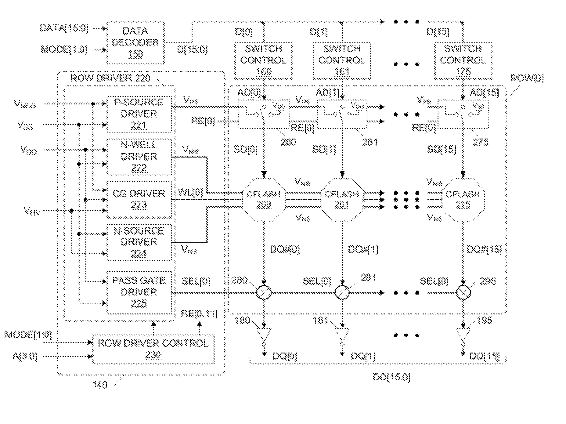
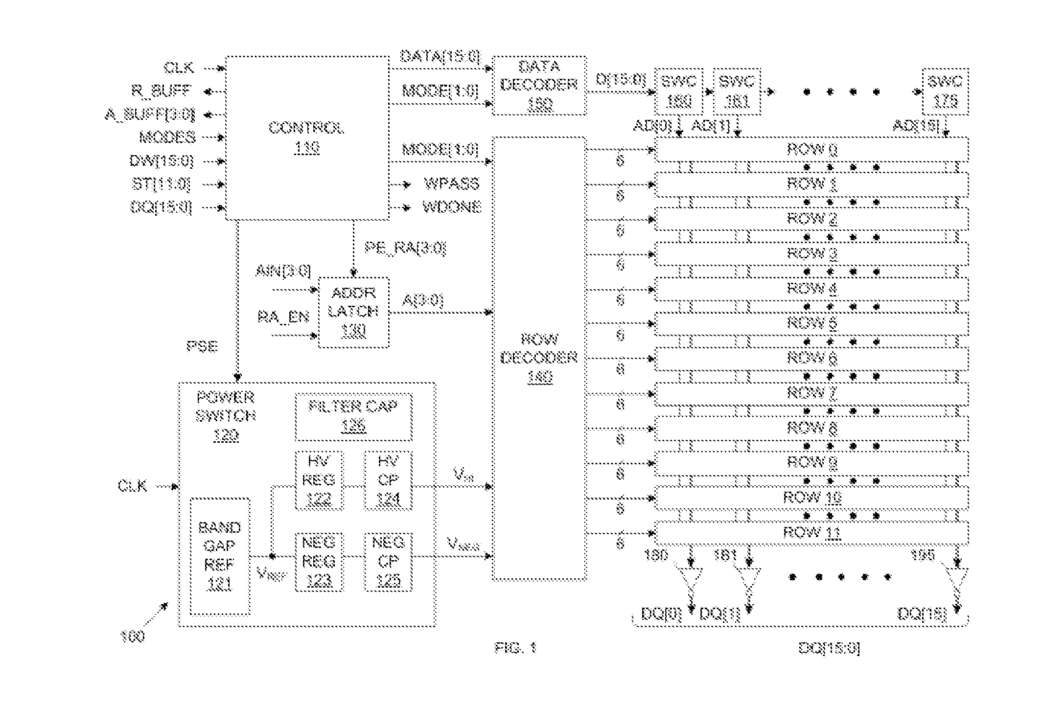
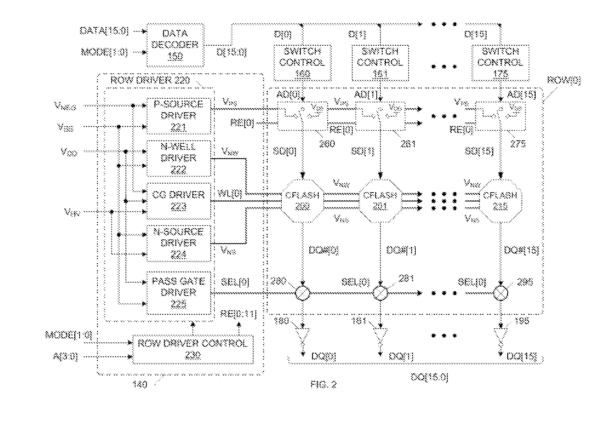
[0010]FIG. 1 is a block diagram of an ultra-low power non-volatile memory (NVM) module 100 in accordance with one embodiment of the present invention. NVM module 100 includes control circuit 110, power switch 120, address latch 130, row decoder 140, data decoder 150, switch control circuits 160-175, output inverters 180-195 and NVM rows 0-11. In the described examples, each of NVM rows 0-11 includes sixteen compact flash memory cells, such that NVM module 100 includes a total of 192 compact flash memory cells (12 rows×16 columns). Other embodiments can include different numbers of rows and columns. In accordance with the described embodiments, the compact flash memory cells used in NVM module 100 are described in U.S. Pat. No. 6,788,576, which is incorporated herein by reference. In other embodiments, other compact flash memory cells may be used. In the described embodiments, NVM module 100 is fabricated using a 0.18 micron process and exhibits a layout area of about 0.095 mm2

[0011...


PUM


Abstract

An improved ultra-low power NVM module, which exhibits low power consumption and reduced layout area. An array of compact flash memory cells are programmed and erased in response to positive and negative boosted voltages. However, the compact flash memory cells are read using conventional supply voltages, thereby minimizing power consumption during a read operation. The ultra-low power NVM module of the present invention can be fabricated using conventional VLSI process steps. The ultra-low power NVM module of the present invention also allows simple operation in all modes (i.e., program, erase, read and standby).

Description

FIELD OF THE INVENTION [0001] The present invention relates to a non-volatile memory module that exhibits an ultra-low power requirement. Such a non-volatile memory module can be used, for example, in radio frequency identification (RFID) applications. BACKGROUND OF THE INVENTION [0002] Many applications, including RFID applications, require non-volatile memory (NVM) modules that exhibit ultra-low power and a small layout area. It would therefore be desirable to have such a NVM module. SUMMARY [0003] Accordingly, the present invention provides an improved ultra-low power NVM module, which exhibits low power consumption and reduced layout area. In accordance with one embodiment of the present invention, an array of compact flash memory cells are programmed and erased in response to positive and negative boosted voltages (while the supply voltage is 1.8 Volts to 2.2 Volts). However, the compact flash memory cells are read using conventional supply voltages (e.g., 1 Volt to 2.2 Volts),...

Claims


Application Information

Patent Timeline
IPC IPC(8): G11C16/04G11C11/34G11C16/06
CPCG11C5/04G11C16/12G11C16/045G11C16/0441
Inventor SARIG, EREZ
Owner RPX CORP
Learn More