Method of Fabricating Light Emitting Device and Thus-Fabricated Light Emitting Device

Inactive Publication Date: 2007-09-27
SHIN-ETSU HANDOTAI CO LTD
View PDF12 Cites 42 Cited by
  • Summary
  • Abstract
  • Description
  • Claims
  • Application Information

AI Technical Summary

Benefits of technology

[0044] On the other hand, when the light emitting layer section is understood as a collective of a large number of point light sources arrayed in plane as shown in FIG. 11, beam of light from each of the point light sources is emitted as spreading omni-directionally. Assuming now the normal line drawn from each point light source down onto the light extraction surface, it is geometrically obvious that any components of the beam of light emitted at angles not smaller than α, away from the normal line, will cause angle of incidence again not smaller than α on the light extraction surface, so far as the surface is a flat plane, so that the light returns back into the layer by total reflection. Accordingly, as for the main light extraction area and the side-face light extraction areas of the GaP transparent semiconductor layer, we can assume similar circular cones having the point light source at the apex thereof, around the normal line drawn from the point light source down onto the individual areas. Of all components of incident beam directed from each point light source towards the individual areas, the components extractable out to the external are limited to those fallen inside the circular cones (the circular cones are referred to as escape cones). On the other hand, formation of the surface roughening projections on the light extraction area can largely increase the ratio of extractable beam of light incident at low angles, when considered on the basis of substantial angle of incidence on the irregularities, and can also increase the surface area of that area by virtue of the irregularities, so that even components of the beam of light fallen outside the escape cones now become extractable in an effective manner from the planar area.
[0045] Critical angle α of total reflection is a determinant of the apex angle of the extraction cone (or escape cone), wherein the angle α is as small as 17 to 27° at most as described in the above. On the main surface on the light extraction side of the light emitting layer section, the ratio of area sectioned by the extraction cones standing on the point light sources becomes scarce, and also the ratio of components of the incident light falling outside the extraction cones and returned back into the layer becomes large. The reflected light may, however, be able to escape from the side faces of the GaP transparent semiconductor layer after repeating internal reflection. Square chips can use all of four side faces of the GaP transparent semiconductor layer as the light extraction areas, so that it is critically important to improve the light extraction efficiency from the side faces of the layer. Formation of the surface roughening projections on the side faces can therefore largely improve the light extraction efficiency of the light emitting device as a whole.
[0046] Any excessive residue of process-induced damage layer formed in the side-face light extraction areas of the GaP transparent semiconductor layer after the dicing not only inhibits smooth formation of the surface roughening projections by the succeeding chemical etching, but also allows a part of the process-induced damage to remain even after the formation of the surface roughening projections, possibly causative of absorption or scattering of the beam of emitted light. It is therefore effective to etch off, after the dicing, the process-induced damage layer formed in the side-face light extraction areas of the GaP transparent semiconductor layer, using a damage-removing solution composed of an aqueo

Problems solved by technology

Conventional efforts have been made on increasing the energy of light extraction by effectively spreading current within the device through consideration on geometry of the electrode, but increase in the electrode area is inevitable anyhow in this case, having been fallen in a dilemma that a smaller light extraction area results in a limited energy of light extraction.
Another problem resides in that the current is less likely to spread in the in-plane direction, because the dopant carrier concentration, and consequently the conductivity ratio, of the cladding layer is suppressed to a slightly lower level in order to optimize emissive recombination of carriers in the active layer.
This results in concentration of the current into the region covered by the electrode, and consequently lowers the substantial energy of light extraction from the light leakage region.
However investigatio

Method used


Image

  • Method of Fabricating Light Emitting Device and Thus-Fabricated Light Emitting Device
  • Method of Fabricating Light Emitting Device and Thus-Fabricated Light Emitting Device
  • Method of Fabricating Light Emitting Device and Thus-Fabricated Light Emitting Device

Examples


Example

[0081] Paragraphs below will describe best modes for carrying out this invention referring to the attached drawings.

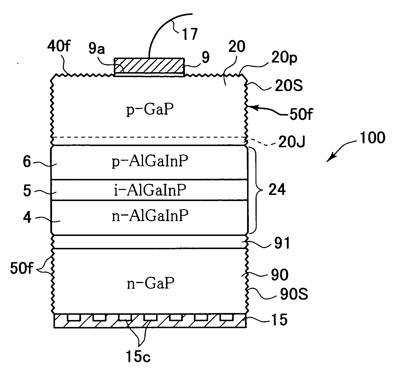
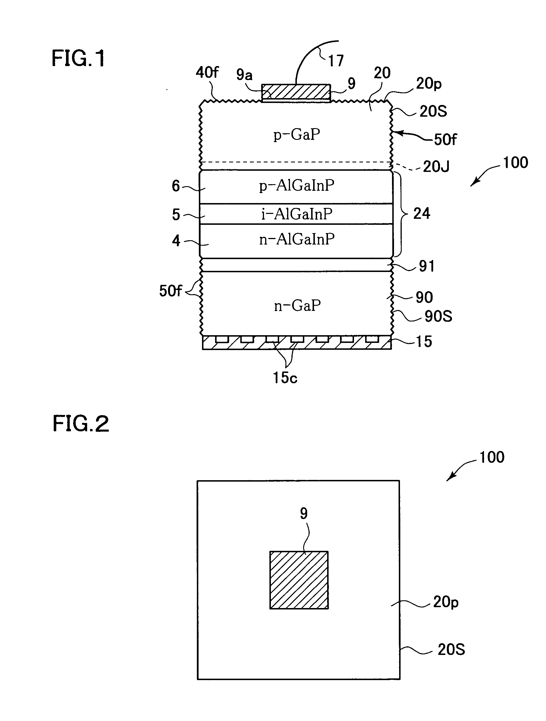
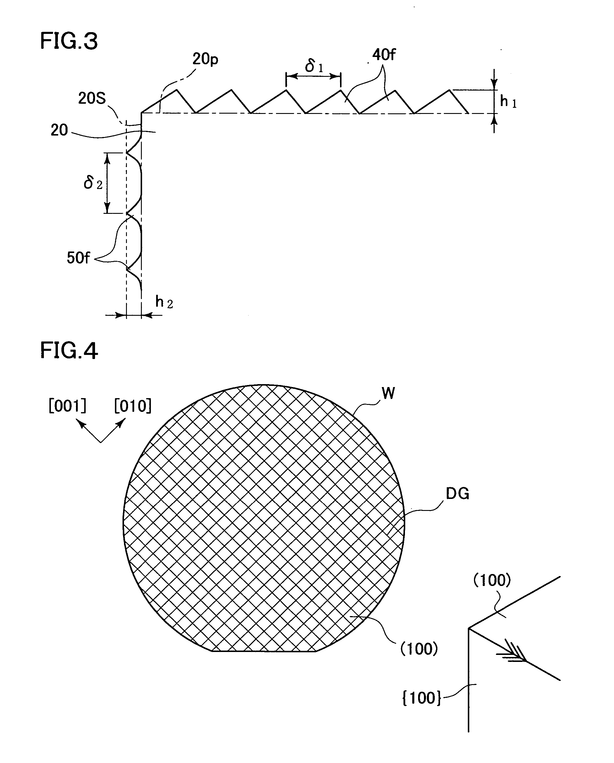
[0082]FIG. 1 is a conceptual drawing of a light emitting device 100 as one embodiment of this invention. The light emitting device 100 has a light emitting layer section 24 composed of a III-V compound semiconductor, and a GaP light extraction layer (p-type herein) as a first GaP transparent semiconductor layer, formed on a first main surface side of the light emitting layer section 24. On a second main surface side of the light emitting layer section 24, a GaP transparent substrate layer 90 as a second GaP transparent semiconductor layer is disposed. In this embodiment, a chip of the light emitting device 100 has a plain geometry of 300-μm square.

[0083] The light emitting layer section 24 has a structure in which an active layer 5 composed of a non-doped (AlxGa1-2)yIn1-yP alloy (where, 0≦x≦0.55, 0.45≦y≦0.55) is held between a p-type cladding layer (first-conductivit...


PUM


Abstract

A light emitting device chip is obtained by dicing a light emitting device wafer having a light emitting layer section 24 based on a double heterostructure in which a first-conductivity-type cladding layer 6, an active layer 5 and an second-conductivity-type cladding layer 4, each of which being composed of a compound semiconductor having a composition allowing lattice matching with GaAs, out of compound semiconductors expressed by formula (AlxGa1-x)yIn1-yP (where, 0≦x≦1, 0≦y≦1), are stacked in this order, and having the (100) surface appeared on the main surface thereof, and GaP transparent semiconductor layers 20, 90 stacked on the light emitting layer section 24 as being agreed with the crystal orientation thereof, so that the {100} surfaces appear on the side faces of the GaP transparent semiconductor layer. Accordingly, there can be provided a method of fabricating a light emitting device having the AlGaInP light emitting layer section and the GaP transparent semiconductor layers, less causative of failures such as edge chipping during the dicing.

Description

RELATED APPLICATIONS [0001] This application claims the priority of Japanese Patent Application No. 2004-131807 filed on Apr. 27, 2004, which is incorporated herein by reference. BACKGROUND OF THE INVENTION [0002] 1. Field of the Invention [0003] This invention relates to a method of fabricating a light emitting device and thus-fabricated light emitting device. [0004] 2. Description of the Related Art [0005] Light emitting device having the light emitting layer section thereof composed of an (AlxGa1-x)yIn1-yP alloy (where, 0≦x≦1, 0≦y≦1; simply referred to as AlGaInP alloy, or more simply as AlGaInP, hereinafter) can be realized as a high-luminance device over a wide wavelength range typically from green region to red region, by adopting a double heterostructure in which a thin AlGaInP active layer is sandwiched between an n-type AlGaInP cladding layer and a p-type AlGaInP cladding layer, both having a larger band gap. Current is supplied to the light emitting layer section through a...

Claims


Application Information

Patent Timeline
IPC IPC(8): H01L33/00H01L33/16H01L21/308H01L33/30
CPCH01L33/0079H01L33/30H01L33/22H01L33/0095H01L33/0093
Inventor IKEDA, HITOSHISUZUKI, KINGONAKAMURA, AKIO
Owner SHIN-ETSU HANDOTAI CO LTD
Why Eureka
Try Eureka