Unit cell of semiconductor integrated circuit and wiring method and wiring program using unit cell

a technology of integrated circuits and unit cells, applied in the field of unit cells of semiconductor integrated circuits and wiring methods and wiring programs using unit cells, can solve the problems of logic cells not being wired, the degree of integration consequently declines, and the wiring efficiency declines

Inactive Publication Date: 2007-10-04
SOCIONEXT INC
View PDF9 Cites 34 Cited by
  • Summary
  • Abstract
  • Description
  • Claims
  • Application Information

AI Technical Summary

Benefits of technology

[0022]Moreover, the upper-layer wiring region is formed, in a unit cell, at a predetermined position in the first direction. Therefore, when a plurality of unit cells are arranged in a matrix to construct a functional circuit block, between the unit cells that contact with each other in the second direction, the upper-layer wiring regions are positioned on an identical horizontal grid in the second direction, and the upper-layer wiring regions contact with each other. Th...

Problems solved by technology

Then, since signal wiring formed on the second metal wiring layer and various signal wirings formed on the third metal wiring layer are obstructed by the stacked vias, wiring efficiency declines, which is a problem.
In addition, when the auxiliary power wiring 104 is wired on the second metal wiring layer, logic cells cannot be wired since signal wiring is obstructed by the auxiliary power wiring 104, and the degree of integration consequently declines, which is a probl...

Method used


Image

  • Unit cell of semiconductor integrated circuit and wiring method and wiring program using unit cell
  • Unit cell of semiconductor integrated circuit and wiring method and wiring program using unit cell
  • Unit cell of semiconductor integrated circuit and wiring method and wiring program using unit cell

Examples


Embodiment Construction

[0029]Semiconductor integrated circuit devices have been designed by an automatic arranging / wiring system employing a calculator or the like. An automatic arranging / wiring method includes a standard cell type as a representative. In the standard cell type, basic gates and frequently-used logic circuit patterns are first registered in a cell library as unit cells. Then, arrangement of the unit cells and multilayer wiring between the cells are carried out based on a netlist of the semiconductor integrated circuit device so that an automatic arrangement design is completed.

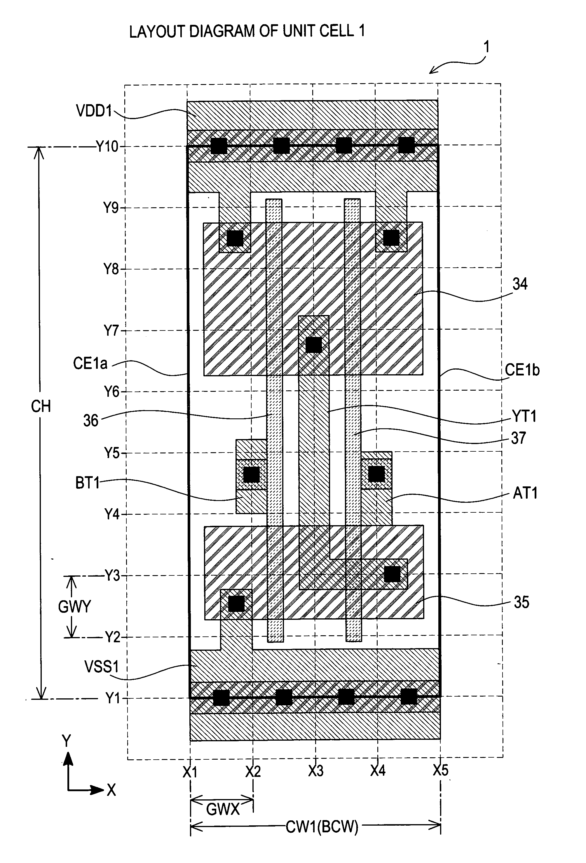
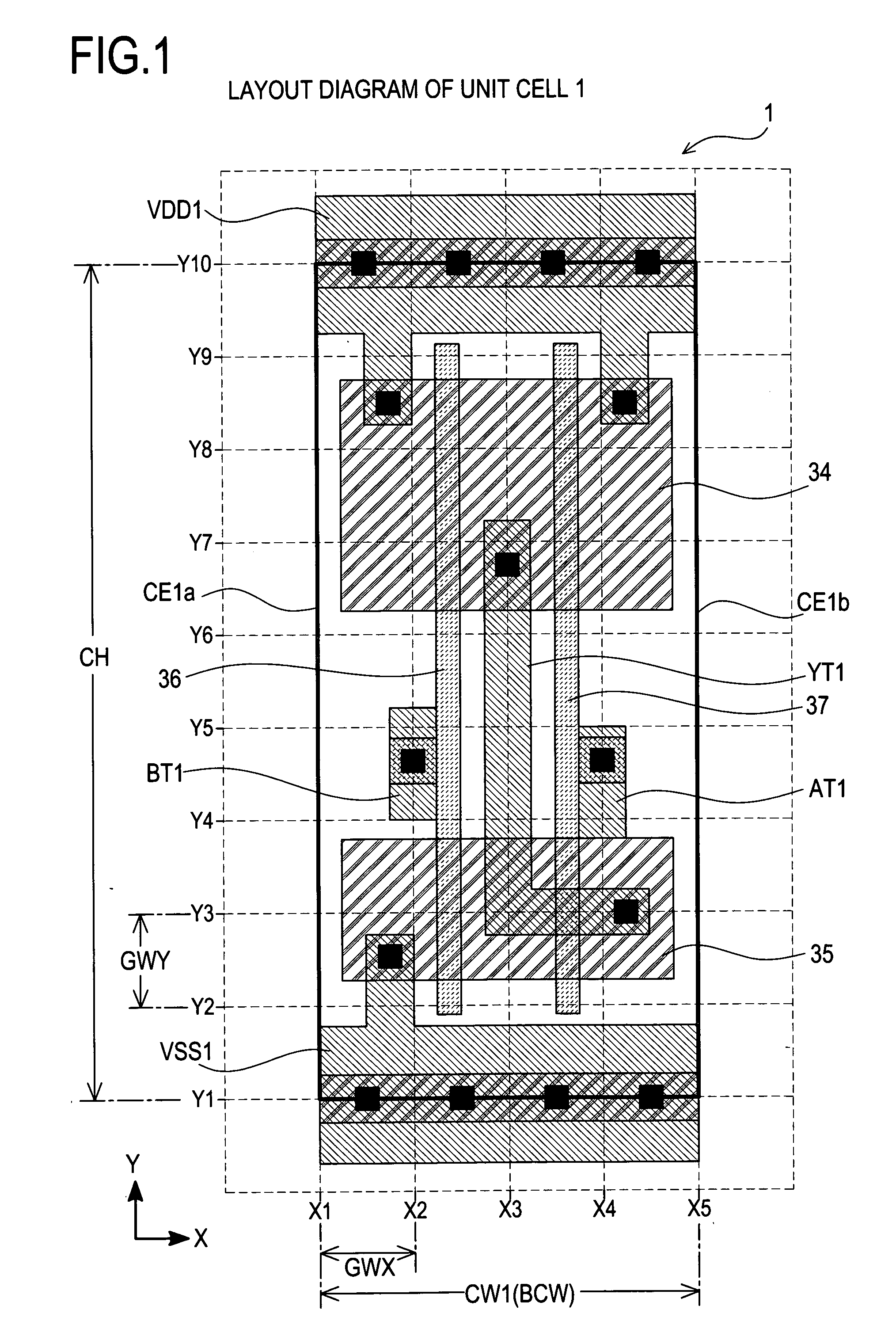
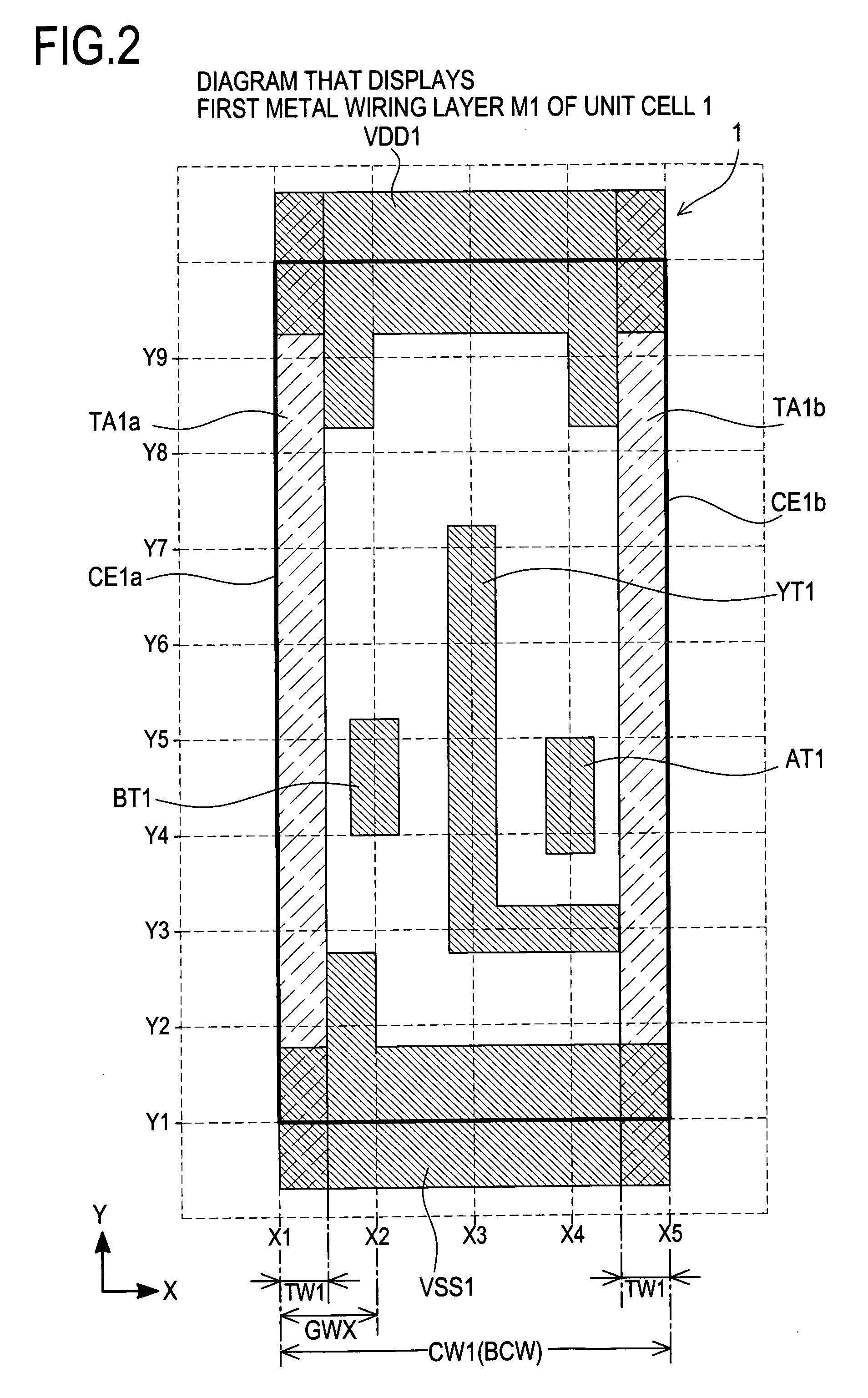
[0030]An embodiment of the present invention will be described in detail by use of FIG. 1 to FIG. 4. Unit cells according to the present embodiment are characterized in that the cell widths of all unit cells registered in the cell library have been unified at integral multiples of a basic cell width BCW. Here, for example, unit cells that can be formed with cell widths narrower than the basic cell width BCW (for exam...


PUM


Abstract

A unit cell of a semiconductor integrated circuit capable of improving wiring efficiency in layout of a functional circuit block or the like using a unit cell, and a wiring method and wiring program using the unit cell are provided. In a unit cell, auxiliary power wiring regions are formed with reference to grids that exist from a cell edge every basic cell width in the X-direction. Input signal terminals and an output signal terminal are each arranged so as to include at least one wiring connecting portion outside the auxiliary power wiring regions. This makes it possible to wire wiring other than signal wiring in the auxiliary power wiring region. When a functional circuit block is constructed by arranging unit cells in a matrix, auxiliary power wiring regions are formed at a pitch of the basic cell width, through the functional circuit block in the Y-direction.

Description

CROSS-REFERENCE TO RELATED APPLICATIONS[0001]This application is based upon and claims the benefit of priority from each of the prior Japanese Patent Application No. 2006-098218 filed on Mar. 31, 2006, the entire contents of which are incorporated herein by reference.BACKGROUND OF THE INVENTION[0002]1. Field of the Invention[0003]The present invention relates to a unit cell that forms a fundamental unit in a layout of a semiconductor integrated circuit device and further to a wiring method and wiring program using the unit cell, and more particularly, it relates to a unit cell that is used for a gate array type or standard cell type semiconductor integrated circuit device and a wiring method and wiring program using the unit cell.[0004]2. Description of Related Art[0005]Conventionally, semiconductor integrated circuit devices by a gate array type, a standard cell type, and the like for which functional circuit blocks formed by arranging unit cells are arranged in a matrix have exist...

Claims


Application Information

Patent Timeline
IPC IPC(8): H01L27/10
CPCH01L27/11807H01L27/0207
Inventor KOMAKI, MASAKI
Owner SOCIONEXT INC
Why Eureka
Try Eureka