

Exposure apparatus and device manufacturing method
a technology of exposure apparatus and manufacturing method, which is applied in the direction of photomechanical treatment, printing, instruments, etc., can solve the problems of reducing the accuracy of exposure, and the precision of focus detection in the exposure area becomes a problem
- Summary
- Abstract
- Description
- Claims
- Application Information
AI Technical Summary
Benefits of technology
Problems solved by technology
Method used
Image

Examples
Embodiment Construction
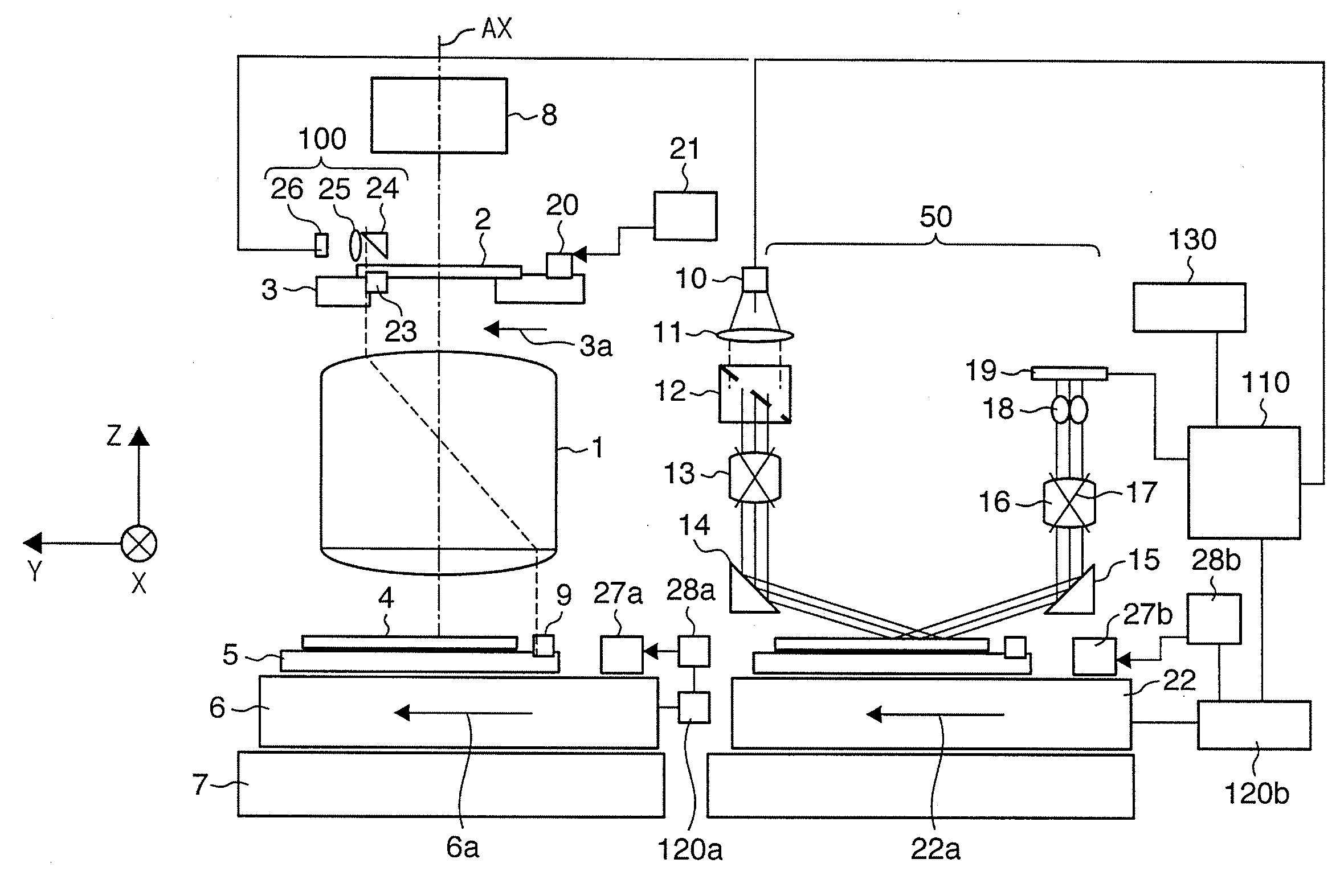
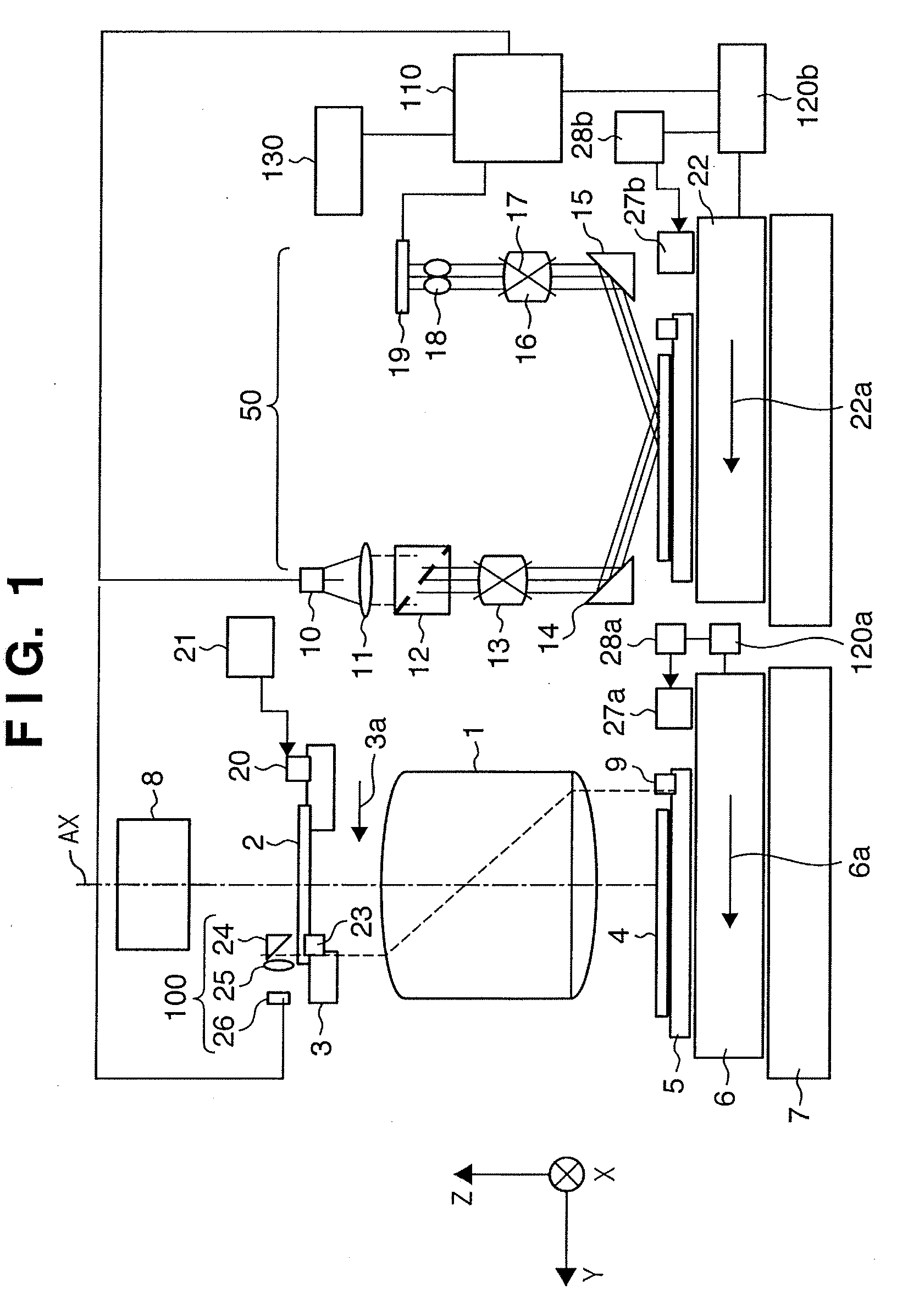
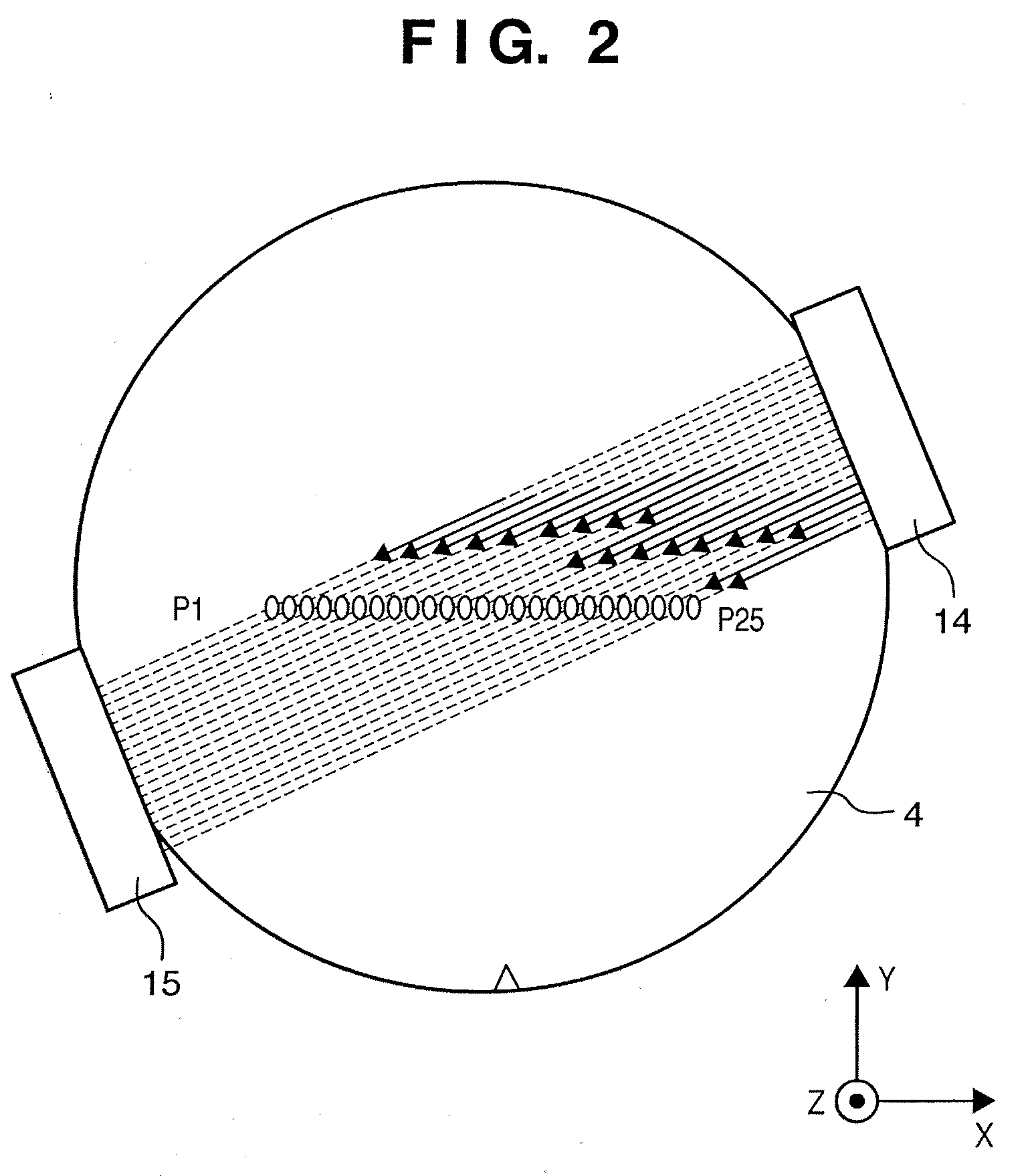
[0030]Embodiments of the present invention will now be described in detail with reference to the accompanying drawings. The embodiments reduce a disadvantage, such as local defocusing, caused by variations in the positional relationship between shot regions and measurement points among a plurality of shot regions.
[0031]FIG. 1 shows the overall configuration of an exposure apparatus according to an exemplary embodiment of the present invention. An example is described applied to a scanning exposure apparatus.
[0032]A scanning is driven with a reticle 2 having a pattern held by an reticle stage 3. The reticle 2 is output from an illumination optical system 8, and illuminated by a slit light obtained by being formed by a slit member. Thus, an image of the pattern of the reticle 2 is formed in the image plane of a projection optical system 1 by the slit light. A substrate (wafer) 4 on which a photosensitive agent (photoresist) has been applied is positioned in the image plane. Below, the...
PUM
 Abstract
Description
Claims
Application Information