Piezoelectric MEMS switch and method of fabricating the same

a technology of micro-electromagnetic system and switch, which is applied in the direction of manufacturing tools, generators/motors, devices, etc., can solve the problems of deteriorating productivity, high driving voltage to apply, and uniform performance of mems switches, so as to improve the degree of freedom in process design

Inactive Publication Date: 2007-10-04
SAMSUNG ELECTRONICS CO LTD
View PDF5 Cites 6 Cited by
  • Summary
  • Abstract
  • Description
  • Claims
  • Application Information

AI Technical Summary

Benefits of technology

[0018]Exemplary embodiments of the present invention address at least the above aspects. Accordingly, an aspect of the present invention is to provide a piezoelectric MEMS switch in which a piezoelectric actuator is formed prior to RF signal lines, thereby removing a process of unreasonably etching an undersurface of a substrate and improving a degree of freedom in process design.

Problems solved by technology

Thus, there arises a problem that a high driving voltage should be applied to the movable electrode to drive the movable electrode.
Thus, a gap between the fixed electrode and the movable electrode is not uniform, but different according to the MEMS switches, thereby uniformity in performances of the MEMS switches being deteriorated.
Also, the conventional MEMS switch requires a large number of fabrication processes, thereby a productivity being deteriorated.
In addition, the conventional MEMS switch is disadvantageous in that a contact force of the contact member is unstable, and a contact loss is increased as the contact member repeats the switching operation.
However, according to the conventional piezoelectric RF MEMS switch 20, there are a lot of difficulties in fabrication.
More particularly, a fabrication process is complicated.

Method used


Image

  • Piezoelectric MEMS switch and method of fabricating the same
  • Piezoelectric MEMS switch and method of fabricating the same
  • Piezoelectric MEMS switch and method of fabricating the same

Examples


Embodiment Construction

[0054]Reference will now be made in detail to exemplary embodiments of the present invention, which are illustrated in the accompanying drawings, wherein like reference numerals refer to the like elements throughout. The exemplary embodiments are described below in order to explain the present invention by referring to the figures.

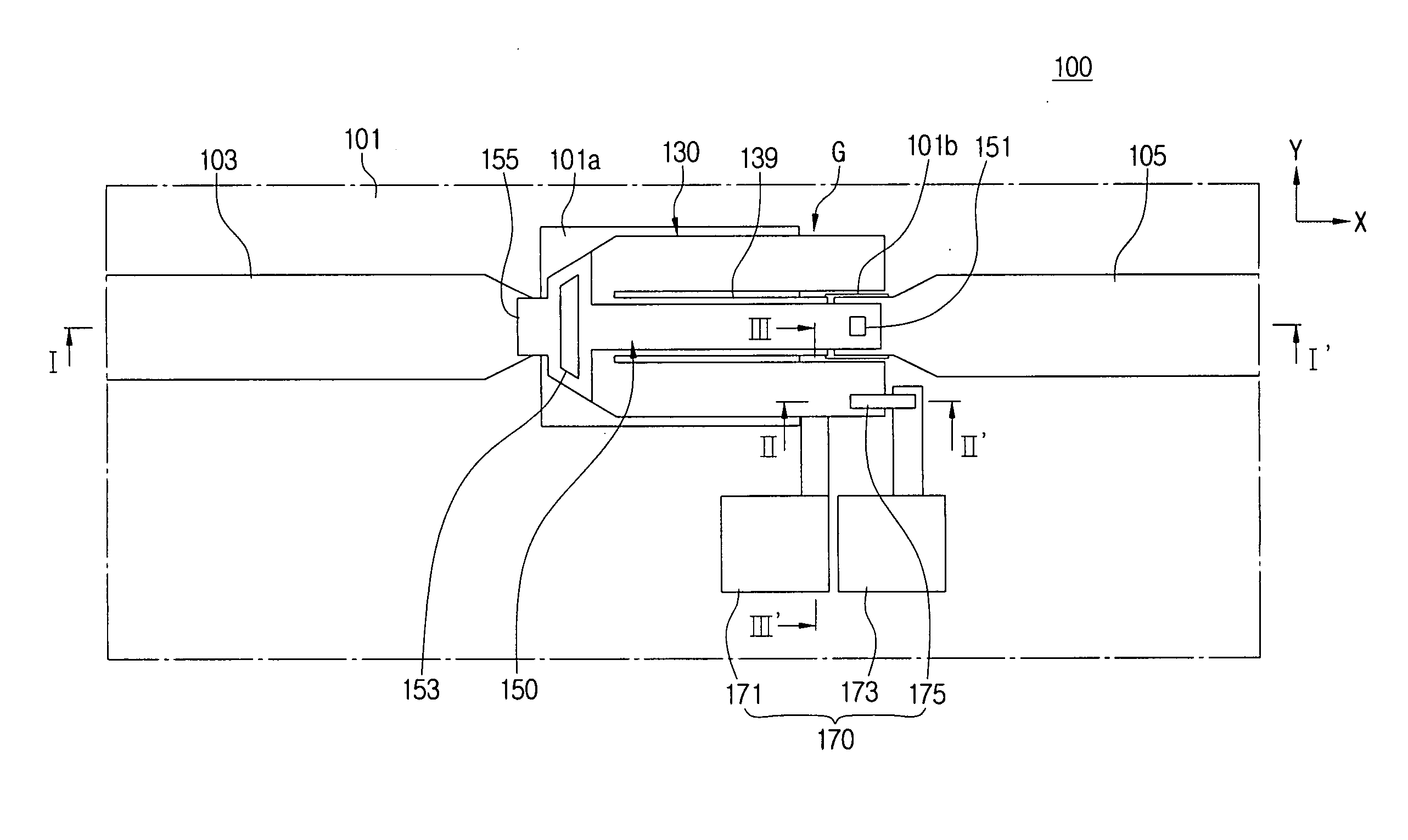
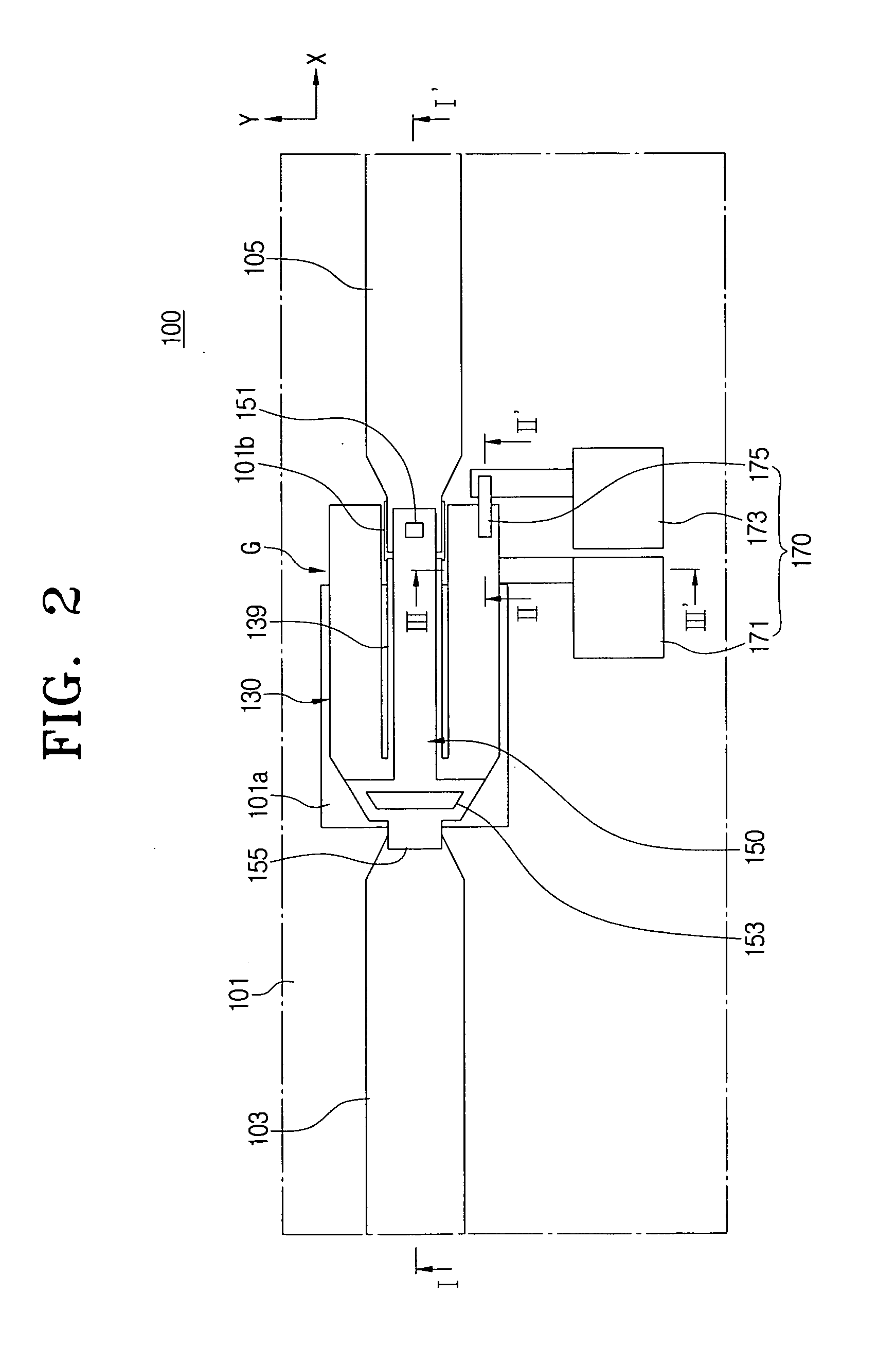
[0055]FIG. 2 is a top plan view exemplifying a piezoelectric MEMS switch in accordance with an exemplary embodiment of the present invention, FIG. 3A is a cross-sectional view taken along line I-I′ of FIG. 2, and FIG. 3B is a cross-sectional view exemplifying the piezoelectric MEMS switch of FIG. 3A when it is operated.

[0056]Referring to FIGS. 2 through 3B, the piezoelectric MEMS switch in accordance with the exemplary embodiment of the present invention includes a substrate 101, first and second fixed signal lines 103 and 105, a piezoelectric actuator 130, and a movable signal line 150.

[0057]The first and the second fixed signal lines 103 and 105 are symm...


PUM

PropertyMeasurementUnit
voltageaaaaaaaaaa
lengthaaaaaaaaaa
lengthaaaaaaaaaa

Abstract

A piezoelectric Micro Electro Mechanical System (MEMS) switch includes a substrate, first and second fixed signal lines symmetrically formed in a spaced-apart relation to each other on the substrate to have a predetermined gap therebetween, a piezoelectric actuator disposed in alignment with the first and the second fixed signal lines in the predetermined gap, and having a first end supported on the substrate to allow the piezoelectric actuator to be movable up and down, and a movable signal line having a first end connected to one of the first and the second fixed signal lines, and a second end configured to be in contact with, or separate from the other of the first and second fixed signal lines, the movable signal line at least one side thereof being connected to an upper surface of the piezoelectric actuator.

Description

CROSS-REFERENCE TO RELATED PATENT APPLICATION[0001]This application claims priority under 35 U.S.C. § 119 (a) from Korean Patent Application No. 10-2006-0028991 filed on Mar. 30, 2006 in the Korean Intellectual Property Office, the disclosure of which is incorporated herein by reference.BACKGROUND OF THE INVENTION[0002]1. Field of the Invention[0003]Apparatuses and methods consistent with the present invention relate to a Micro Electro Mechanical System (MEMS) switch, such as a Radio Frequency (RF) switch, fabricated using a MEMS technique, and in particular, to a MEMS switch which is driven by using a piezoelectric element or actuator, and a method of fabricating the same.[0004]2. Description of the Related Art[0005]Recently, a lot of electronic systems, which are used at a high frequency band, are tending to reduce a weight to an ultra lightweight, to decrease a size to an ultra small size, and to enhance a performance in a high level. Accordingly, an ultra small-sized micro switc...

Claims


Application Information

Patent Timeline
Patent Type & Authority Applications(United States)
IPC IPC(8): B25G3/28B81B3/00B81C1/00H01H49/00H01H57/00H01L41/09H01L41/18H01L41/22H01L41/29H02N2/00
CPCH01H57/00Y10T403/7026H01H2057/006B81B3/00B81B7/02B81C1/00
Inventor KIM, JONG-SEOKSONG, IN-SANGLEE, SANG-HUNKWON, SANG-WOOKLEE, CHANG-SEUNGHONG, YOUNG-TACKKIM, CHE-HEUNG
Owner SAMSUNG ELECTRONICS CO LTD
Why Eureka
Try Eureka