Converter circuit for switching of a multiplicity of switching voltage levels

Inactive Publication Date: 2007-10-11
ABB RES LTD
View PDF5 Cites 17 Cited by
  • Summary
  • Abstract
  • Description
  • Claims
  • Application Information

AI Technical Summary

Benefits of technology

[0007] The p second switching groups and p third switching groups that are provided, as well as their connections as described above, mean, for example, that the p second switching groups are involved in the phase output AC voltage only in the positive half-cycle, and the p third switching groups are involved in the phase output AC voltage only during the negative half-cycle, during operation of the converter circuit according to the invention. This advantageously makes it possible to reduce the amount of electrical energy which is stored in the converter circuit, in particular in the capacitors in the p second and third switching groups. Furthermore, the n first switching groups are used only for balancing of the phase output AC voltage, so that, when a plurality of first switching groups are present, the capacitors in t

Problems solved by technology

One problem with a converter circuit for switching of a multiplicity of switching voltage levels according to DE 692 05 413 T2 is that the electrical energy that is stored in the converter circuit during operation is very high.
However, this results in physically large capacitors, which are correspondingly expensive.
Furthermore, the

Method used


Image

  • Converter circuit for switching of a multiplicity of switching voltage levels
  • Converter circuit for switching of a multiplicity of switching voltage levels
  • Converter circuit for switching of a multiplicity of switching voltage levels

Examples


first embodiment

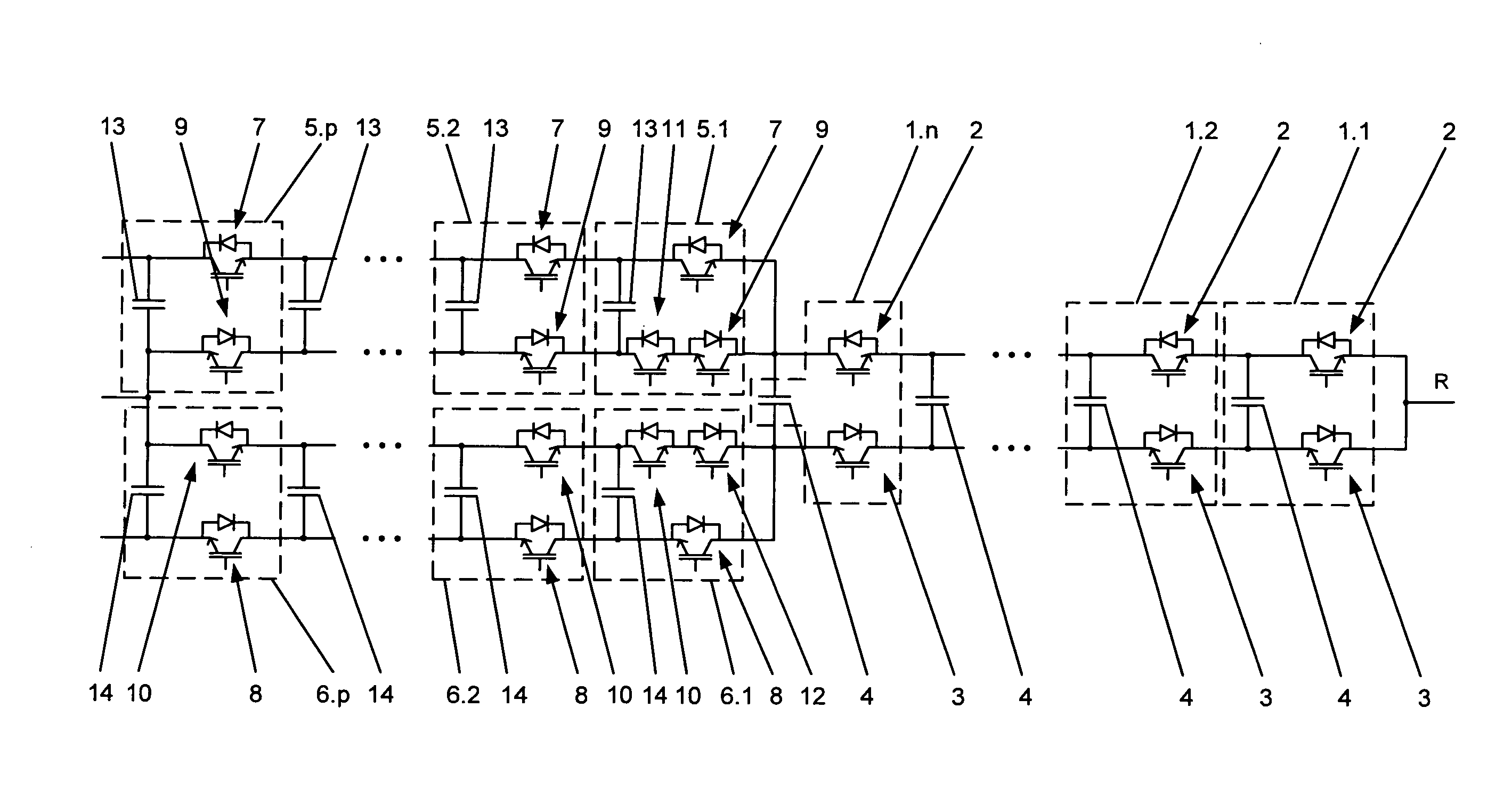
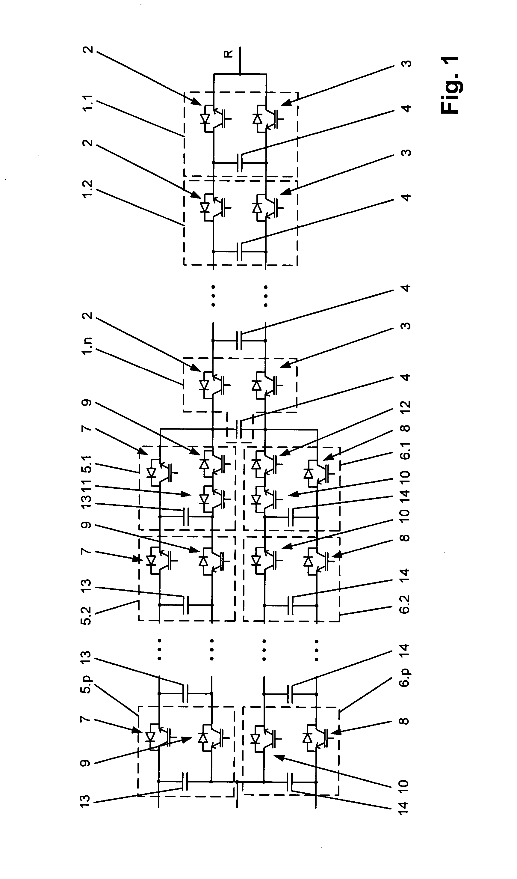
[0010]FIG. 1 shows a converter circuit according to the invention,

second embodiment

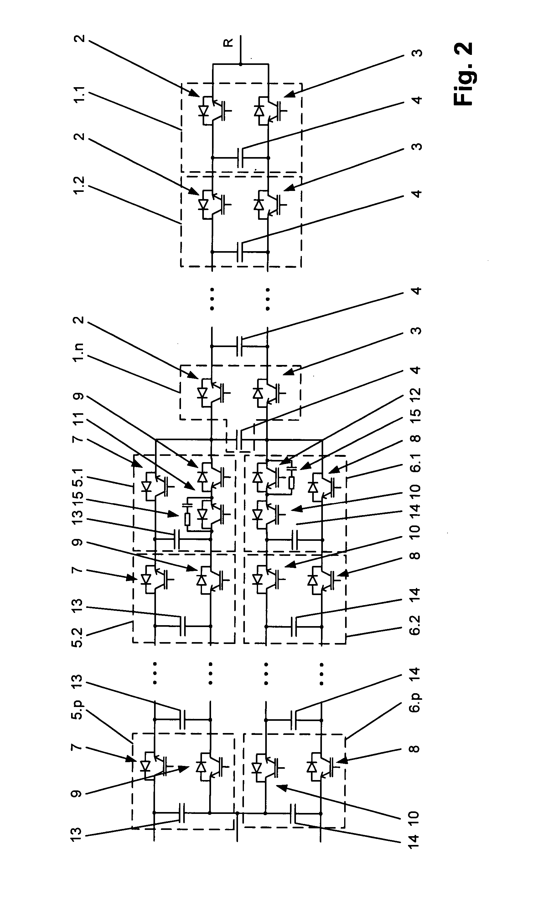
[0011]FIG. 2 shows a converter circuit according to the invention, and

third embodiment

[0012]FIG. 3 shows a converter circuit according to the invention.

[0013] The reference symbols used in the drawings and their meanings are listed in summarized form in the list of reference symbols. In principle, identical parts are provided with the same reference symbols in the figures. The described embodiments represent examples of the subject matter of the invention, and have no restrictive effect.

Approaches to Implementation of the Invention

[0014]FIG. 1 shows one embodiment, in particular a single-phase embodiment, of a converter circuit according to the invention for switching of a multiplicity of switching voltage levels. In this case, the converter circuit has n first switching groups 1.1, . . . , 1.n which are provided for each phase R, Y, B, with the n-th first switching group 1.n being formed by a first drivable bidirectional power semiconductor switch 2 and a second drivable bidirectional power semiconductor switch 3, and with the first first switching group 1.1 to t...


PUM


Abstract

A converter circuit is specified for switching of a multiplicity of switching voltage levels, which have n first switching groups (1.1, . . . , 1.n) for each phase (R, S, T), with the n-th first switching group (1.n) being formed by a first drivable bidirectional power semiconductor switch (2) and a second drivable bidirectional power semiconductor switch (3), and with the first first switching group (1.1) to the (n−1)-th switching group (1.(n−1)) each being formed by a first drivable bidirectional power semiconductor switch (2) and a second drivable bidirectional power semiconductor switch (3), and by a capacitor (4) which is connected to the first and second drivable bidirectional power semiconductor switches (2, 3) with each of the n first switching groups (1.1, . . . , 1.n) being connected in a linked form to the respectively adjacent first switching group (1.1, . . . , 1.n), and with the first and the second drivable bidirectional power semiconductor switches (2, 3) in the first first switching group (1.1) being connected to one another. In order to reduce the stored electrical energy in the converter circuit, n≧1, and p second switching groups (5.1, . . . , 5.p) and p third switching groups (6.1, . . . , 6.p) are provided, which each have a first drivable bidirectional power semiconductor switch (7, 8), a second drivable bidirectional power semiconductor switch (9, 10) and a capacitor (13, 14), where p≧1. Each of the p second switching groups (5.1, . . . , 5.p) is connected in a linked form to the respectively adjacent second switching group (5.1, . . . , 5.p), and each of the p third switching groups (6.1, . . . , 6.p) is connected in a linked form to the respectively adjacent third switching group (6.1, . . . , 6.p). Furthermore, the first second and the first third switching group (5.1, 6.1) each have a third drivable bidirectional power semiconductor switch (11, 12) which is connected back-to-back in series with the respective second drivable bidirectional power semiconductor switch (9, 10), with the first second switching group (5.1) being connected to the first drivable bidirectional power semiconductor switch (2) in the n-th first switching group (1.n), and with the first third switching group (6.1) being connected to the second drivable bidirectional power semiconductor switch (3) in the n-th first switching group (1.n), and the capacitor (13) in the p-th second switching group (5.p) is connected in series with the capacitor (14) in the p-th third switching group (6.p).

Description

TECHNICAL FIELD [0001] The invention relates to the field of power electronics, and relates in particular to a converter circuit for switching of a multiplicity of switching voltage levels, as claimed in the preamble of the independent claim. PRIOR ART [0002] Nowadays, a wide range of converter circuits are used for power-electronic applications. The requirements for a converter circuit such as this are in this case on the one hand to produce as few harmonics as possible in phases of an electrical AC power supply system which is normally connected to the converter circuit, and on the other hand to transmit power levels that are as high as possible with as small a number of electronic components as possible. One suitable converter circuit for switching of a multiplicity of switching voltage levels is specified in DE 692 05 413 T2. n first switching groups are provided for each phase in this document, with the n-th first switching group being formed by a first power semiconductor swit...

Claims


Application Information

Patent Timeline
IPC IPC(8): H01H9/54H02M7/48H02M7/49
CPCH02M7/483H02M7/49H02M7/4833
Inventor STEIMER, PETERBARBOSA, PETERMEYSENC, LUC
Owner ABB RES LTD
Why Eureka
Try Eureka