Load control device having a variable drive circuit

a variable drive circuit and control device technology, applied in the direction of incandescent lamp energy saving, pulse technique, sustainable building, etc., can solve the problems of increasing emi noise, phase-control output will have many high-frequency components, and significant increase in total power dissipation

Active Publication Date: 2007-10-11
LUTRON TECH CO LLC
View PDF30 Cites 40 Cited by
  • Summary
  • Abstract
  • Description
  • Claims
  • Application Information

AI Technical Summary

Problems solved by technology

Accordingly, a small increase in the switching time tSWITCH can cause a significant rise in the total power dissipation PD-TOTAL of the FETs.
If the switching time tSWITCH, i.e., the time when the semiconductor switch changes from the conductive state to the nonconductive state (and vice versa), is substantially short, the phase-control output will have many high-frequency components and the EMI noise will be increased.
However, the increased switching times tSWITCH due to the gate resistor RG lead to an increased total power dissipation PD-TOTAL of the FET (as shown in Equation 2 above).
Further, as the power dissipation PD-TOTAL of the FET increases and the temperature of the FET rises, the on-resistance RDS(on) will increase, which then leads to an increased conduction loss PD-CONDUCT.
Compounding this thermal issue is the fact that the rising temperature causes the internal characteristics of the FET to change such that the threshold voltage VTH of the FET decreases.
This condition can lead to a thermal runaway situation, which causes undesirable device temperatures and, ultimately, failure of the FETs (for example, when the temperature of the FETs rises to 135° C.).
However, this causes the intensity level of the lighting load to change, which is undesirable.

Method used


Image

  • Load control device having a variable drive circuit
  • Load control device having a variable drive circuit
  • Load control device having a variable drive circuit

Examples


second embodiment

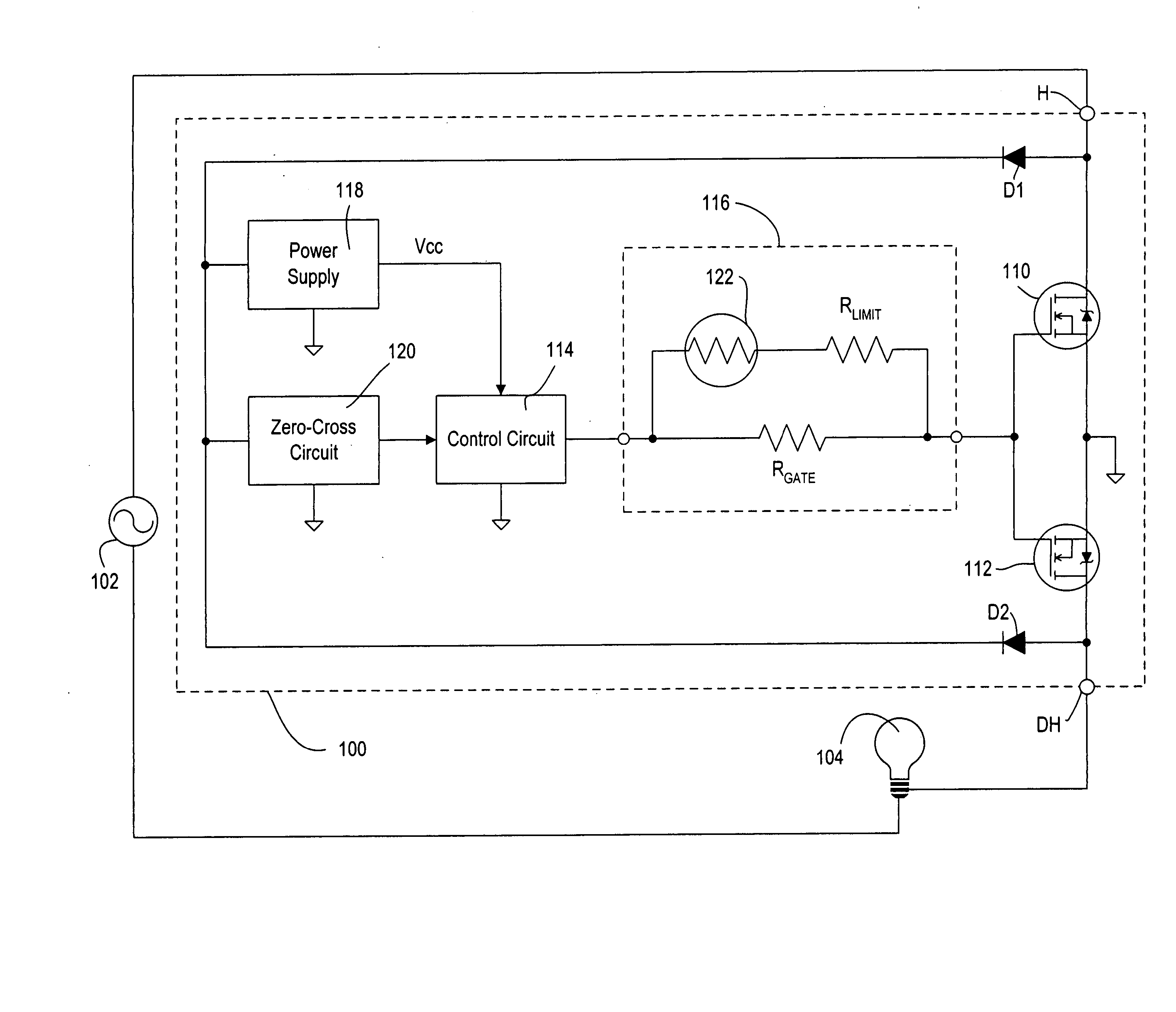
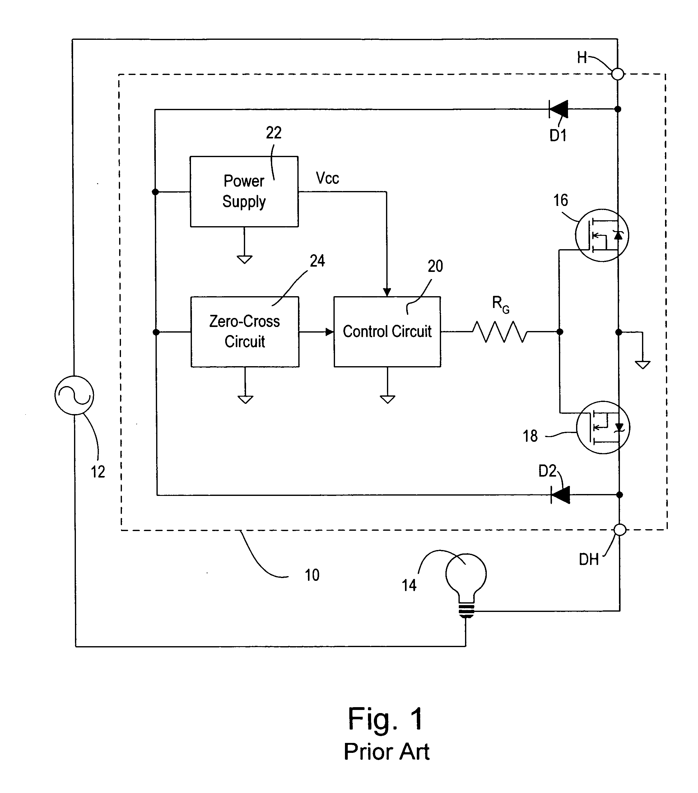
[0035]FIG. 5 is a simplified schematic diagram of a dimmer 150 having two variable gate drive circuits 116A, 116B according to the present invention. A control circuit 114A is operable to individually control each of the FETs 110, 112. The first variable drive circuit 116A is provided in series between the control circuit 114A and the gate of the first FET 110 and is thermally coupled to the first FET 110. Similarly, the second variable gate drive circuit 116B is provided in series between the control circuit 114A and the gate of the second FET 112 and is thermally coupled to the second FET 112. Each of the variable gate drive circuits 116A, 116B operate in a similar fashion to the single variable gate drive circuit 116 of the dimmer 100 shown in FIG. 3 to provide a continuously variable impedance in series with the gates of each of the FETs 110, 112. Preferably, the first variable drive circuit 116A is only responsive to the temperature of the first FET 110, while the second variab...

third embodiment

[0036]FIG. 6 is a simplified schematic diagram of a dimmer 200 according to the present invention. The dimmer 200 includes a variable drive circuit 216 that is operable to provide a plurality of discrete steps of different impedances in series between a control circuit 214 and the gates of the FETs 110, 112. The variable drive circuit 216 includes a plurality of resistors 230-239 in parallel electrical connection. Each of the resistors 230-239 is coupled in series electrical connection with a controllably conductive device 240-249, respectively. The controllably conductive devices 240-249 may each comprise a FET or an IGBT in a full-wave rectifier bridge, two FETs or IGBTs in anti-series connection, or any other suitable type of bidirectional switch.

[0037] The controllably conductive devices 240-249 each have control inputs, which are coupled to the control circuit 214 such that the control circuit is operable to selectively couple the resistors 230-239 in series with the gates of t...


PUM


Abstract

A load control device for controlling the amount of power delivered to an electrical load from a source of AC power comprises a controllably conductive device and a variable gate drive circuit. The controllably conductive device is coupled in series electrical connection between the source and the electrical load to control the amount of power delivered to the load. The variable drive circuit is thermally coupled to the controllably conductive device and provides a continuously variable impedance in series with the control input of the controllably conductive device. The impedance of the variable drive circuit is operable to decrease as a temperature of the controllably conductive device increases and vice versa. Preferably, the variable drive circuit comprises an NTC thermistor. Accordingly, the switching times of the controllably conductive device, i.e., the times when the controllably conductive device is changing between the conductive and non-conductive states, remain constant, or alternatively decrease, as the temperature of the controllably conductive device increases.

Description

FIELD OF THE INVENTION [0001] The present invention relates to drive circuits for controllably conductive devices in load control devices, and, more particularly, to temperature-sensitive drive circuits for semiconductor switches, such as field-effect transistors (FETs), in electric light dimmers. BACKGROUND OF THE INVENTION [0002] Standard load control devices, such as electric light dimmers, use one or more semiconductor switches, such as triacs or field-effect transistors (FETs), to control the current delivered to an electric load, for example, to control the intensity of a lighting load. The semiconductor switch is typically coupled in series between an alternating-current (AC) source and the lighting load. Using a phase-control dimming technique, the dimmer renders the semiconductor switch conductive for a portion of each half-cycle to provide power to the lighting load, and renders the semiconductor switch non-conductive for the other portion of the half-cycle to disconnect p...

Claims


Application Information

Patent Timeline
Patent Type & Authority Applications(United States)
IPC IPC(8): H05B39/04
CPCH02M1/44H02M5/293H03K2217/0009Y02B20/148H05B39/048Y02B20/00
Inventor DAVIS, GREGORY T.ORCHOWSKI, NEILHAUSMAN, DONALD F. JR.
Owner LUTRON TECH CO LLC
Why Eureka
Try Eureka